Light-emitting device having triplet and singlet compound in light-emitting layers

a light-emitting device and compound technology, applied in the direction of discharge tube luminescnet screens, natural mineral layered products, etc., can solve the problems of increasing the kinds of power sources necessary for the light-emitting device, and the shift in the color balance due to the difference in the life (deterioration rate) of the el element, so as to suppress the color balance shift and facilitate circuit design.

Inactive Publication Date: 2008-03-04
SEMICON ENERGY LAB CO LTD
View PDF32 Cites 69 Cited by
  • Summary
  • Abstract
  • Description
  • Claims
  • Application Information

AI Technical Summary

Benefits of technology

[0010]The present invention has been made in view of the above problem, and therefore an object of the present invention is to provide a technique for keeping operation voltages of an EL element with red light emission, an EL element with green light emission and an EL element with blue light emission at a constant level, when a light emitting device is made to perform color display. Another object of the present invention is to provide a light emitting device that can perform color display with good color balance.
[0011]A further object of the present invention is to provide an electric appliance which has a display portion with high image quality, by employing the light emitting device which may perform color display with good color balance as its display portion.
[0020]In the above molecular formulas, M represents an element belonging to Groups 8 to 10 of the periodic table. In the above articles, platinum and iridium are used. Further, the present inventors consider that since nickel, cobalt and palladium are cheaper than platinum and iridium, they are more preferable in reducing the manufacturing cost of the light emitting device. Especially, since nickel can easily form a complex, the productivity is high and therefore preferable.
[0026]However, in the present invention, since the triplet compound with high luminous efficiency is used as the light emitting layer 15 which emits red light, the operation voltages may be made the same whilst the same luminous brightness as the light emitting layer 16 which emits green light and the light emitting layer 17 which emits blue light may be obtained. Accordingly, the deterioration of the light emitting layer 15 which emits red light does not progress significantly, and color display may be performed without causing a problem of shift in color balance, or the like. Further, suppressing the operation voltage as low is preferable also from the point of view that the margin of the withstand pressure of the transistor may be set low.
[0035]As described above, by using the triplet compound and the singlet compound properly, the operation voltages of the EL element which emits red light, the EL element which emits green light and the EL element which emits blue light may all be the same (10 V or less, preferably 3 to 10 V). Accordingly, it is possible to suppress the shift in color balance due to the difference in the life of the EL element, and the power source necessary for the light emitting device may be unified at 3 V or 5 V. Thus, there is an advantage that the circuit design becomes easier.

Problems solved by technology

From the above, it is feared that not only there will be an increase in the kinds of power sources necessary for the light emitting device, but also that a shift in the color balance due to difference in the life (deterioration rate) of the EL element will be generated.

Method used


Image

  • Light-emitting device having triplet and singlet compound in light-emitting layers
  • Light-emitting device having triplet and singlet compound in light-emitting layers
  • Light-emitting device having triplet and singlet compound in light-emitting layers

Examples


embodiment 1

[Embodiment 1]

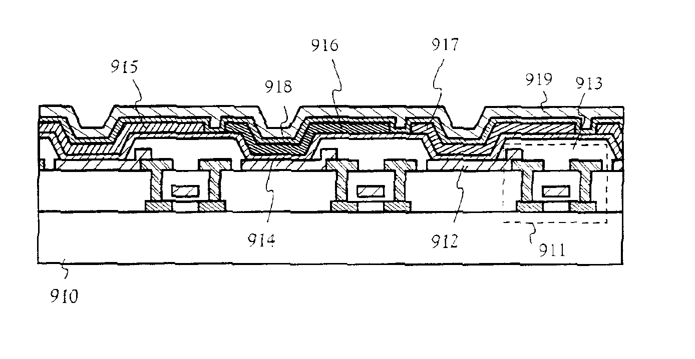
[0051]In this embodiment, as a light emitting device of the present invention, an example of a light emitting device is shown, in which the device has a pixel portion 151 and a driver circuit 150 which drives the pixel portion on the same insulator (however, in a state before seating). Note that, a CMOS circuit as a basic unit is shown for the driver circuit 150, and one pixel is shown for the pixel portion 151. However, in actuality the structure of the pixel portion is made by gathering a plurality of pixels as shown in FIG. 1.

[0052]In FIG. 3, reference numeral 100 indicates an insulator (including an insulating substrate, an insulating film or a substrate having an insulating film on the surface), with an n-channel TFT 201, a p-channel TFT 202, a switching TFT 203 formed of an n-channel TFT, and a current controlling TFT 204 formed of a p-channel TFT formed thereon. At this time, the circuit structure of the pixel portion is the structure shown in FIG. 2A. Further, ...

embodiment 2

[Embodiment 2]

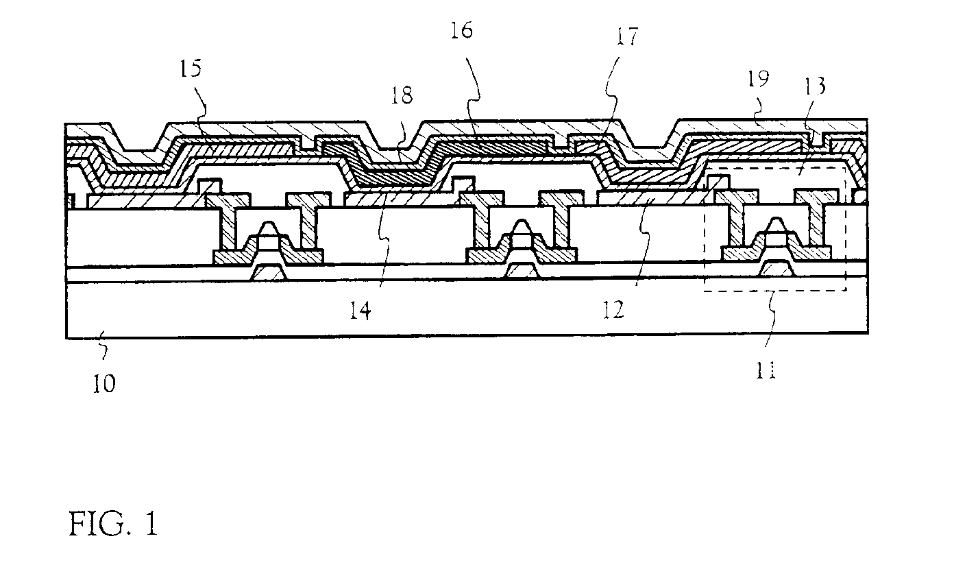
[0069]In this embodiment, as a light emitting device of the present invention, an example of a light emitting device is shown, in which the device has a pixel portion and a driver circuit which drives the pixel portion on the same insulator (however, in a state before sealing). Note that, a CMOS circuit as a basic unit is shown for the driver circuit 250, and one pixel is shown for the pixel portion 251. However, in practice the structure of the pixel portion is made as shown in FIG. 1. Further, the portions with the same symbols attached as FIG. 3 may refer to the description of Embodiment 1.

[0070]In FIG. 4, reference numeral 100 indicates the insulator, with the n-channel TFT 201, the p-channel TFT 202, a switching TFT 206 formed of a p-channel TFT, and a current controlling TFT 207 formed of an n-channel TFT formed thereon. At this time, the circuit structure of the pixel portion 251 is the structure shown in FIG. 2B. Further, in this embodiment, the TFTs are all fo...

embodiment 3

[Embodiment 3]

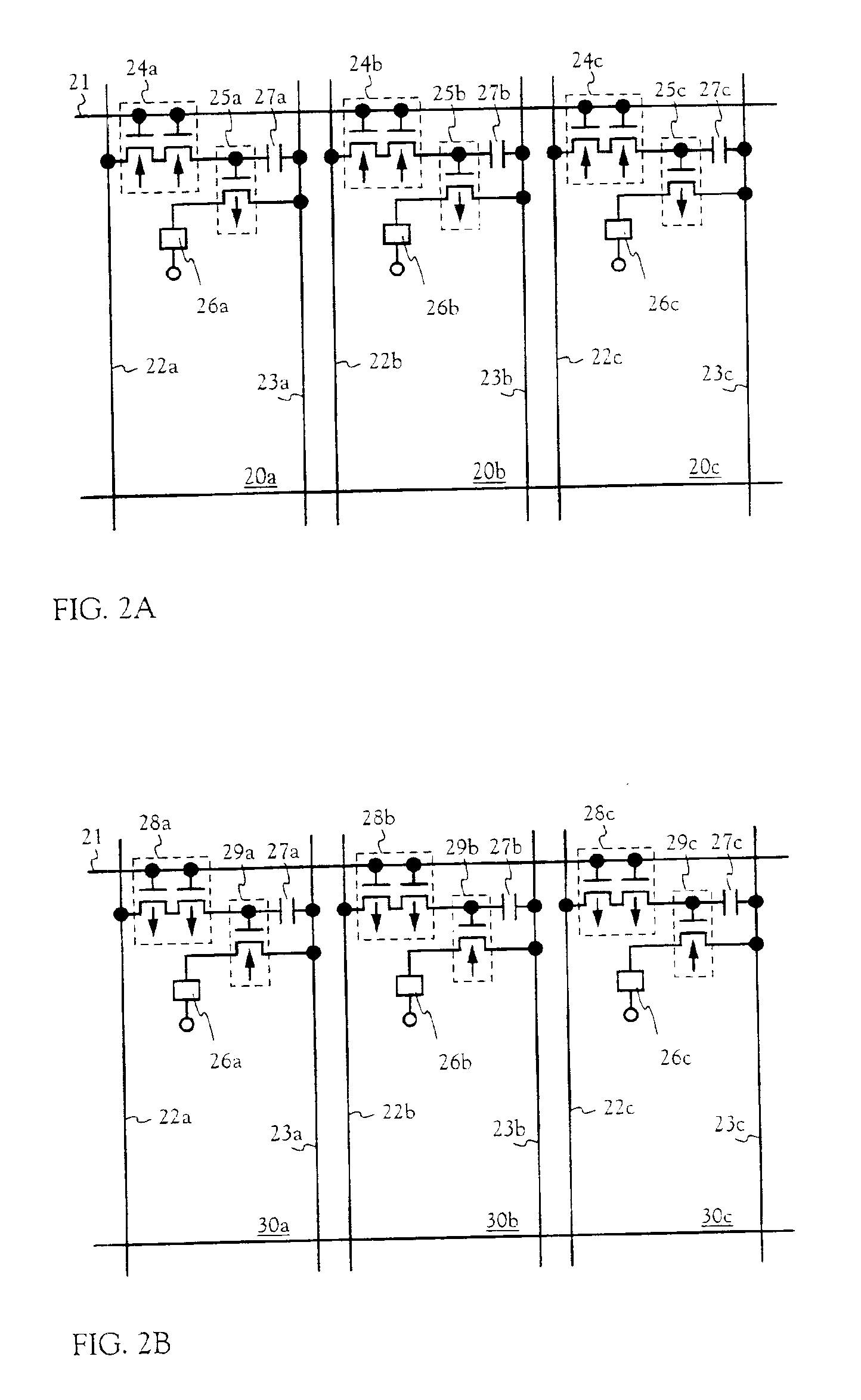
[0079]In this embodiment, as a light emitting device of the present invention, a case where a pixel portion and a driver circuit are all formed of n-channel TFTs is described. Note that, the circuit structure of a pixel of this embodiment is as shown in FIG. 5. Further, the description in FIGS. 2A and 2B may be referred to for portions with the same symbols attached as in FIGS. 2A and 2B.

[0080]As shown in FIG. 5, the switching TFTs 24a to 24c and current controlling TFTs 36a to 36c formed respectively for a pixel (red) 35a, a pixel (green) 35b and a pixel (blue) 35c, are all formed of n-channel TFTs.

[0081]Here the cross sectional structure of the light emitting device of this embodiment (however, in a state before sealing) is shown in FIG. 6. Note that, a CMOS circuit as a basic unit is shown for the driver circuit 350, and one pixel is shown for the pixel portion 351. However, in actuality the structure of the pixel portion 351 is as shown in FIG. 1. Further, for the ...


PUM

PropertyMeasurementUnit
operation voltagesaaaaaaaaaa
temperatureaaaaaaaaaa

Abstract

There is provided a light emitting device which enables a color display with good color balance. A triplet compound is used for a light emitting layer of an EL element that emits red color, and a singlet compound is used for a light emitting layer of an EL element that emits green color and a light emitting layer of an EL element that emits blue color. Thus, an operation voltage of the EL element emitting red color may be made the same as the EL element emitting green color and the EL element emitting blue color. Accordingly, the color display with good color balance can be realized.

Description

BACKGROUND OF THE INVENTION[0001]1. Field of the Invention[0002]The present invention relates to a device (hereinafter, referred to as a light emitting device) having an element (hereinafter, referred to as a light emitting element) sandwiching a luminous material between electrodes. In particular, the present invention relates to a light emitting device having a light emitting element (hereinafter, referred to as an EL element) using an organic compound from which EL (electro luminescence) is obtained as a luminous material. Note that, an organic EL display and an organic light emitting diode (OLED) are included in a light emitting device of the present invention.[0003]Further, the luminous materials that may be used for the present invention include all the luminous materials that luminesce (phosphorescence and / or fluorescence) via a singlet excitation or a triplet excitation, or via both the excitations.[0004]2. Description of the Related Art[0005]In recent years, the development...

Claims


Application Information

Patent Timeline
Patent Type & Authority Patents(United States)
IPC IPC(8): H01J1/62B32B9/00B32B19/00H01L27/32H01L51/00H01L51/30H05B33/00H05B33/14
CPCH01L27/3211H01L27/3244H01L27/3246H01L51/5016H01L51/0085H01L51/0077Y10S428/917H10K59/35H10K59/12H10K85/30H10K85/342H10K50/11H10K2101/10H10K50/828H10K59/122H10K59/123H10K59/1213H10K85/346H10K2102/00H01L27/1214
Inventor YAMAZAKI, SHUNPEI
Owner SEMICON ENERGY LAB CO LTD
Why Eureka
Try Eureka