Semiconductor memory device

a memory device and semiconductor technology, applied in the direction of information storage, static storage, digital storage, etc., can solve the problems of increasing power consumption, unable to apply voltage +3v to the bit line at the time of programming, and unable to apply it to the variable resistance element through the cell access transistor, etc., to achieve the effect of simplifying the manufacturing steps of the semiconductor memory device and reducing the manufacturing cos

Inactive Publication Date: 2008-01-10
SHARP KK
View PDF10 Cites 76 Cited by
  • Summary
  • Abstract
  • Description
  • Claims
  • Application Information

AI Technical Summary

Benefits of technology

[0034]According to the semiconductor memory device in the eleventh characteristics, since the cell access transistor in the memory cell and the transistor constituting the writing mea

Problems solved by technology

However, according to the conventional technique, the voltage +3V applied to the bit line at the time of the programming cannot be applied to the variable r

Method used


Image

  • Semiconductor memory device
  • Semiconductor memory device
  • Semiconductor memory device

Examples


Embodiment Construction

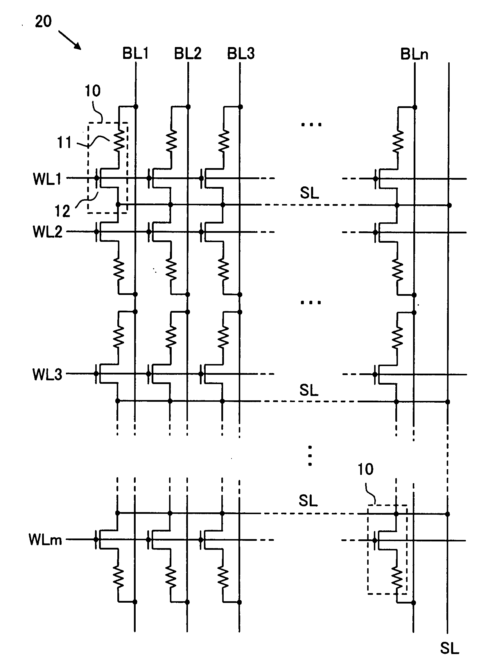
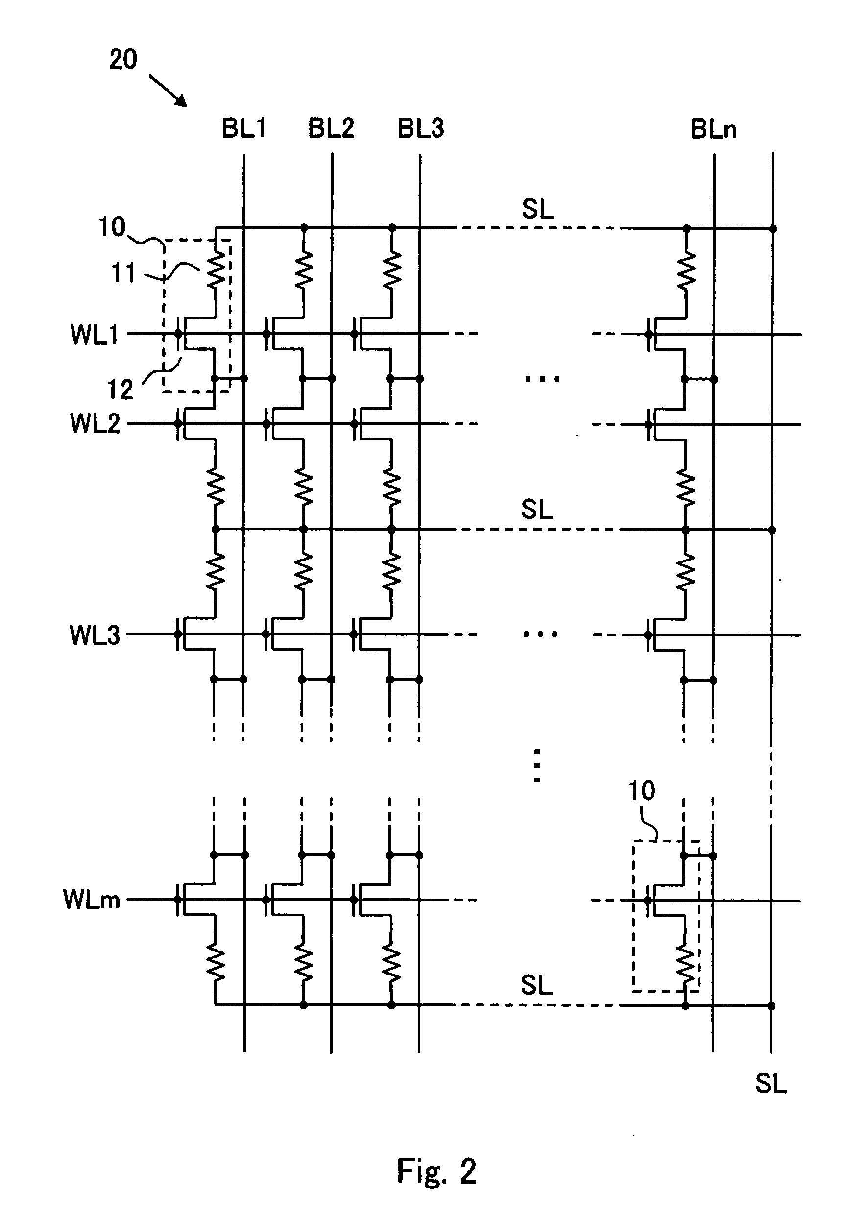
[0049]An embodiment of a semiconductor memory device (referred to as the device of the present invention occasionally hereinafter) according to the present invention will be described with reference to the drawings hereinafter.

[0050]As shown in FIG. 1, the device of the present invention includes one or more memory cell arrays 20 in which a plurality of memory cells 10 are arranged in row and column directions, and, to select a predetermined memory cell or a memory cell group, a plurality of word lines WL1 to WLm and a plurality of bit lines BL1 to BLn are arranged in a row and column directions, respectively and a source line SL extending in the row direction is arranged. In addition, although the source line SL extends in the row direction parallel to the word lines WL1 to WLm and it is provided in each row and connected to other source lines in common outside the memory cell array 20 in FIG. 1, the source line SL may be shred with the two adjacent rows, or it may extend in the co...


PUM


Abstract

A semiconductor memory device comprises writing means for performing a first writing action for shifting an electric resistance of a variable resistance element from a first state to a second state by applying a first voltage between both ends of a memory cell and a gate potential to a gate of a cell access transistor, and a second writing action for shifting the electric resistance from the second state to the first state by applying a second voltage having a polarity opposite to that of the first voltage between both ends of the memory cell and a gate potential to the gate of the cell access transistor, and the polarity and absolute value of the voltage to be applied to both ends of the variable resistance element in the memory cell to be written in the first writing action is different from those in the second writing action.

Description

CROSS REFERENCE TO RELATED APPLICATION[0001]This Nonprovisional application claims priority under 35 U.S.C. §119(a) on Patent Application No. 2006-184654 filed in Japan on 4 Jul., 2006 the entire contents of which are hereby incorporated by reference.BACKGROUND OF THE INVENTION[0002]1. Field of the Invention[0003]The present invention relates to a semiconductor memory device provided with a memory cell including a variable resistance element having two terminals; that can store information by varying its electric resistance between a first state and a second state when voltages having different polarities are separately applied to both ends thereof, and a cell access transistor whose source or drain is connected to one end of the variable resistance element.[0004]2. Description of the Related Art[0005]There has been proposed a method in which one or more short electric pulses are applied to a thin film or bulk formed of a thin film material having Perovskite structure, especially a ...

Claims


Application Information

Patent Timeline
IPC IPC(8): G11C11/00
CPCG11C11/16G11C13/0007G11C13/0069G11C2213/79G11C2213/31G11C2213/32G11C2013/009
Inventor SAITOH, MASAHIROSATO, SHINICHI
Owner SHARP KK
Why Eureka
Try Eureka