Combination readout circuit structure and signal processing readout method of cmos image sensor

An image sensor and readout circuit technology, applied in the field of image sensors, can solve the problems of inability to reduce the speed of the analog output port of the detector, inability to realize pixel merging, limited improvement of the signal-to-noise ratio, etc., so as to avoid the loss of the signal-to-noise ratio and alleviate the Rate pressure, the effect of increasing the working frame rate

Active Publication Date: 2018-10-19
SHANGHAI INST OF TECHNICAL PHYSICS - CHINESE ACAD OF SCI
View PDF4 Cites 0 Cited by
  • Summary
  • Abstract
  • Description
  • Claims
  • Application Information

AI Technical Summary

Problems solved by technology

[0003] However, this method of pixel merging also has significant disadvantages
First of all, CCD pixel merging is based on the accumulation of charge packets. This process cannot be used in the current rapidly developing CMOS detectors; secondly, the maximum number of pixel merging in this way is limited by the capacity of the CCD potential well and cannot be realized. Cell Merging at Any Scale
Although the current CMOS image sensor also has pixel merging technology, it is either accumulated in the digital domain outside the detector, which cannot reduce the speed of the detector’s analog output port, and the signal-to-noise ratio is also limited; or it is limited by the superimposed capacitance. , only a fixed mode (such as 2×2, 4×4) pixel merging can be realized

Method used


Image

  • Combination readout circuit structure and signal processing readout method of cmos image sensor
  • Combination readout circuit structure and signal processing readout method of cmos image sensor
  • Combination readout circuit structure and signal processing readout method of cmos image sensor

Examples


Embodiment Construction

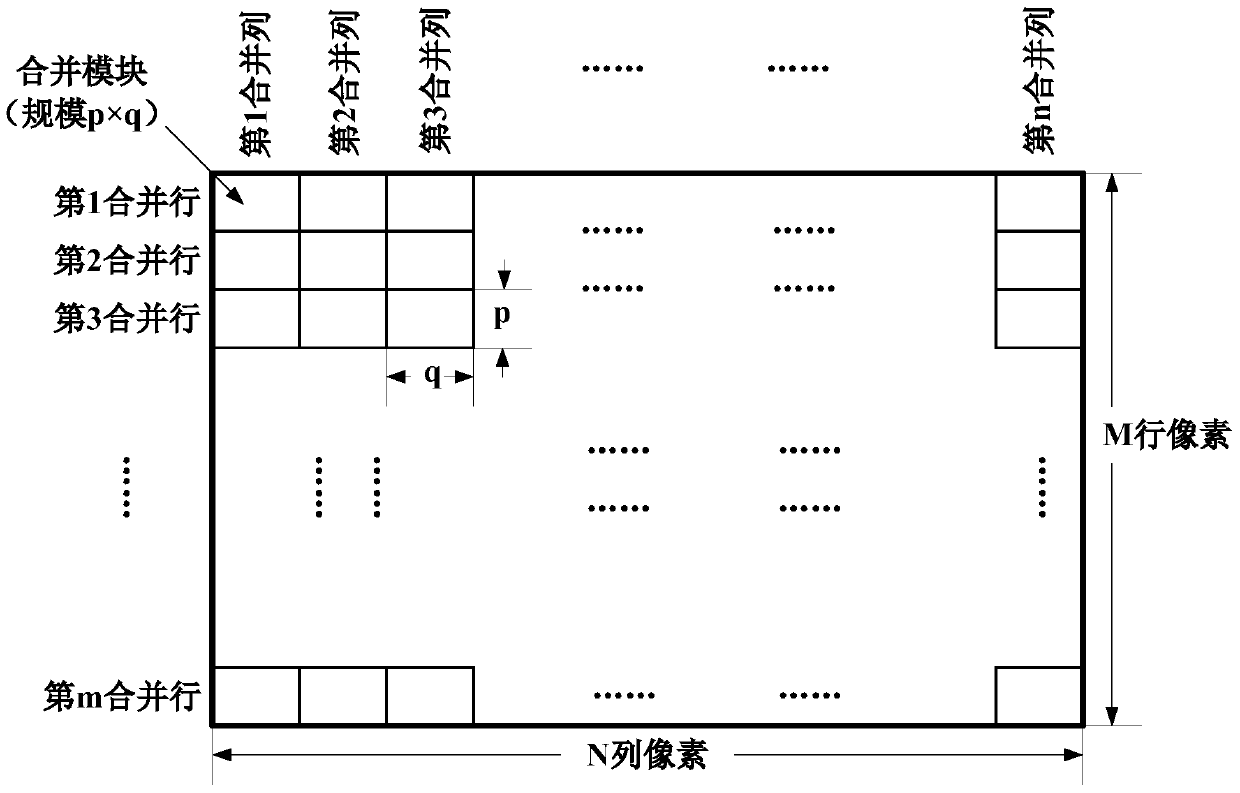
[0026] According to the content of the invention, this embodiment constructs a CMOS detector pixel combination readout structure, the pixel size of the image sensor is 1024×256, 2×2 pixel combination is performed, and the final output size is 512×128.

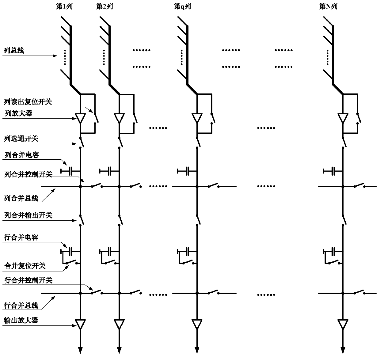
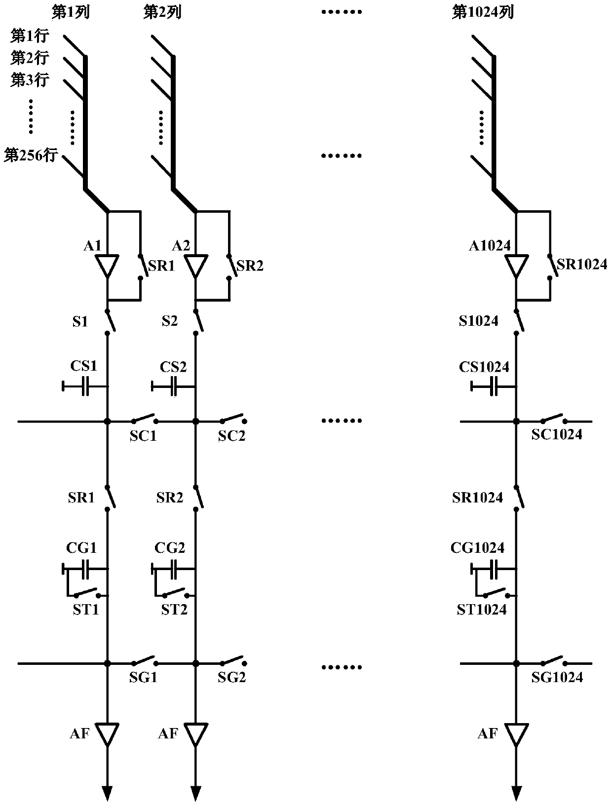
[0027] as attached image 3 As shown, there are 256 rows of detectors in total, and the readout structure includes 1024 column buses, and each column includes column amplifiers (A1~A1024), column gating switches (S1-S1024), column combining capacitors (CS1~CS1024), and column combining Control switch (SC1~SC1024), column merge output switch (SR1~SR1024), row merge capacitor (CG1-CG1024), reset switch (ST1~ST1024), row merge control switch (SG1~SG1024), output amplifier (SG1~ SG1024).

[0028] When the readout structure is changed, the row of the pixels to be merged is sequentially selected by the column bus, and the row and column pixel merge operation is completed through the column merge control switch (SC1~SC1024) and the r...


PUM


Abstract

The invention discloses a combination readout circuit structure and a signal processing readout method of CMOS image sensor picture elements. The structure includes a column bus, a column amplifier, a column readout reset switch, a column gating switch, a column merging capacitor, a column merging control switch, a column merging bus, a column merging output switch, a row merging capacitor, a merging reset switch, and a row merging control switch , line merge bus and output amplifier. When the system is working, the row of pixels to be merged is sequentially selected by the column bus, the row and column pixel merge operation is completed through the column merge control switch and the row merge control switch, and finally the signal after the merged pixels is output through the output amplifier. The invention has the advantages of realizing the combination function of pixels of any scale of the CMOS image sensor, and improving the signal-to-noise ratio and the frame frequency at the same time.

Description

Technical field: [0001] The invention relates to the field of image sensors, in particular to a CMOS image sensor pixel combination readout structure and a signal processing readout method. Background technique: [0002] At present, the performance of CMOS image sensors has been continuously improved, and has been widely used in various scientific imaging, such as remote sensing, high-speed photography, spectral imaging, etc. The specific requirements of such special applications are relatively flexible. Sometimes it is necessary to obtain high-resolution detailed images, and sometimes it is necessary to ensure high frame rate work, and the resolution is not high. In order to solve this problem, the previous CCD image sensor has developed the pixel combination function, which can combine the signals of several adjacent pixels into one and read it out as one pixel. In this way, when a high frame rate is required, this method can be used to sacrifice system resolution, effect...

Claims


Application Information

Patent Timeline
Patent Type & Authority Patents(China)
IPC IPC(8): H04N5/374H04N5/3745H04N5/378
CPCH04N25/766H04N25/77H04N25/75
Inventor 解宁丁毅王欣李梧萤陈世军
Owner SHANGHAI INST OF TECHNICAL PHYSICS - CHINESE ACAD OF SCI
Why Eureka
Try Eureka