The driving circuit of the ito electrode in the lcos display structure
A technology of display structure and driving circuit, which is applied in the application field of electronic technology, can solve the problems of high production cost of LCOS liquid crystal display panel, inability of ITO electrode and metal electrode voltage signals to be completely synchronized, etc.
- Summary
- Abstract
- Description
- Claims
- Application Information
AI Technical Summary
Problems solved by technology
Method used
Image

Examples
Embodiment 1
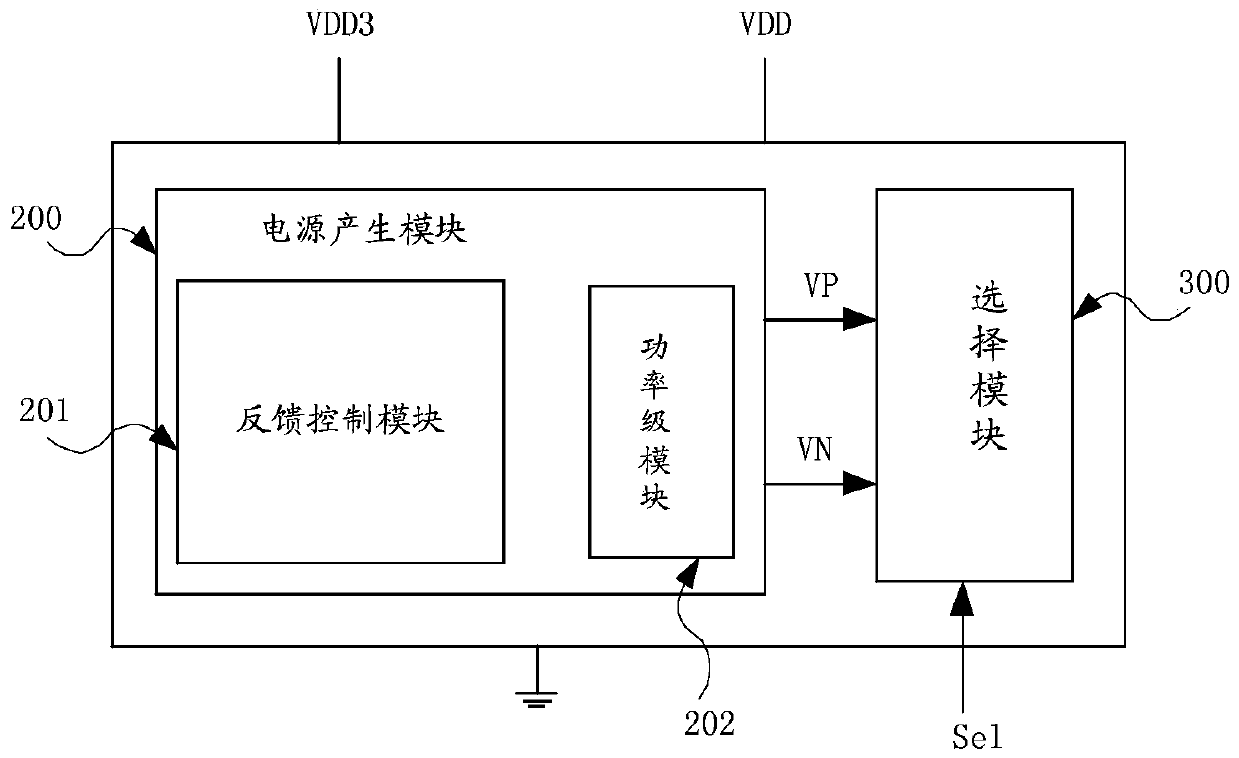
[0066] Embodiments of the present invention provide a driving circuit for ITO electrodes in an LCOS display structure, such as image 3 As shown, it includes a power generation module 200 and a selection module 300, the power generation module 200 is used to generate the voltage required to drive the ITO electrode according to the working voltage of the LCOS display structure, and the selection module 300 is used to generate the voltage according to the power supply The voltage required to drive the ITO electrodes generated by the module 200 generates the driving voltage of the ITO electrodes.
[0067] The operating voltages of the LCOS display structure include: a first operating voltage VDD3 and a second operating voltage VDD, the voltage value of the first operating voltage VDD3 is greater than the voltage value of the second operating voltage VDD. The voltage required to drive the ITO electrode includes: a third working voltage VP and a fourth working voltage VN, and the v...
Embodiment 2
[0094] In this embodiment, the feedback control module 201 includes: a first circuit 2011 , a second circuit 2012 and a third circuit 2013 . The structures of the first circuit 2011 , the second circuit 2012 and the third circuit 2013 are all the same as those in the first embodiment, and will not be repeated here.
[0095] Such as Figure 8As shown, the corresponding power stage module 202 module is not limited to: the first charge pump 401, the second charge pump 402, the sixth capacitor C6 and the seventh capacitor C7; the first charge pump 401 and the second charge pump The clock of the pump 402 is synchronized; the first input end EN of the first charge pump 401 is connected to the output end of the second circuit 2012, the second input end is connected to the first operating voltage VDD3, and the output end is connected to the first operating voltage VDD3. The third working voltage VP is connected to the ground through a sixth capacitor C6; the first input terminal EN o...
PUM
 Abstract
Description
Claims
Application Information