Pixel circuit and display device

A pixel circuit and electrode technology, applied to static indicators, instruments, etc., can solve the problems of large power consumption of display devices, unstable gate potential of drive transistors, and large leakage current of thin-film transistors, etc., to achieve reduced drive frequency, The effect of increasing pixel density and reducing wiring

Active Publication Date: 2019-09-24
HEFEI VISIONOX TECH CO LTD
View PDF5 Cites 27 Cited by
  • Summary
  • Abstract
  • Description
  • Claims
  • Application Information

AI Technical Summary

Problems solved by technology

[0003] An organic light-emitting display device includes a plurality of pixel circuits, and the pixel circuit usually includes a plurality of thin film transistors. In the prior art, the thin film transistors in the pixel circuit are usually formed by a low temperature polysilicon (Low Temperature Poly-silicon, LTPS) process, and the LTPS process is used The leakage current of the formed thin film transistor is large, and the gate potential of the driving transistor is unstable, resulting in large power consumption of the display device

Method used


Image

  • Pixel circuit and display device
  • Pixel circuit and display device
  • Pixel circuit and display device

Examples


Embodiment Construction

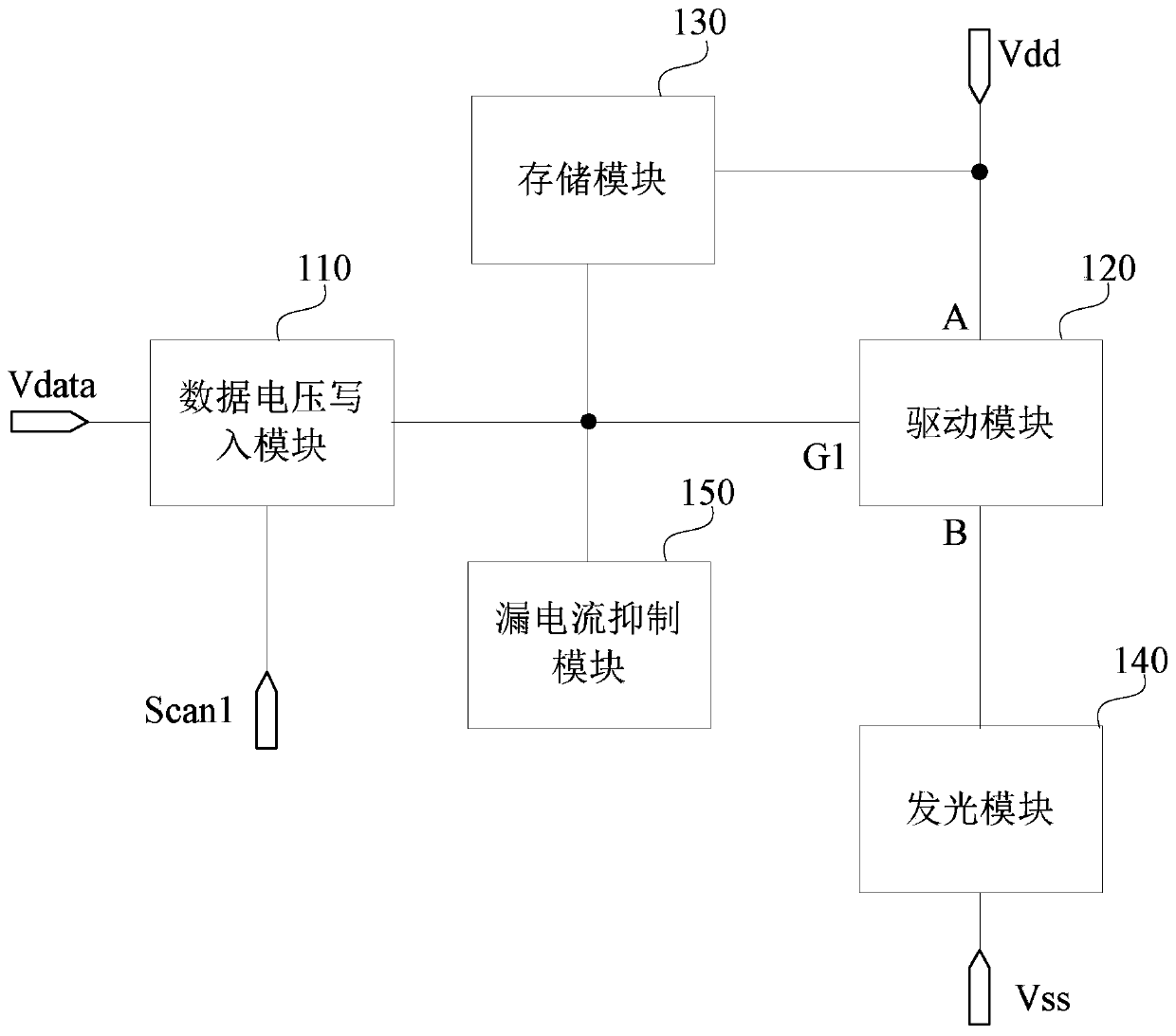
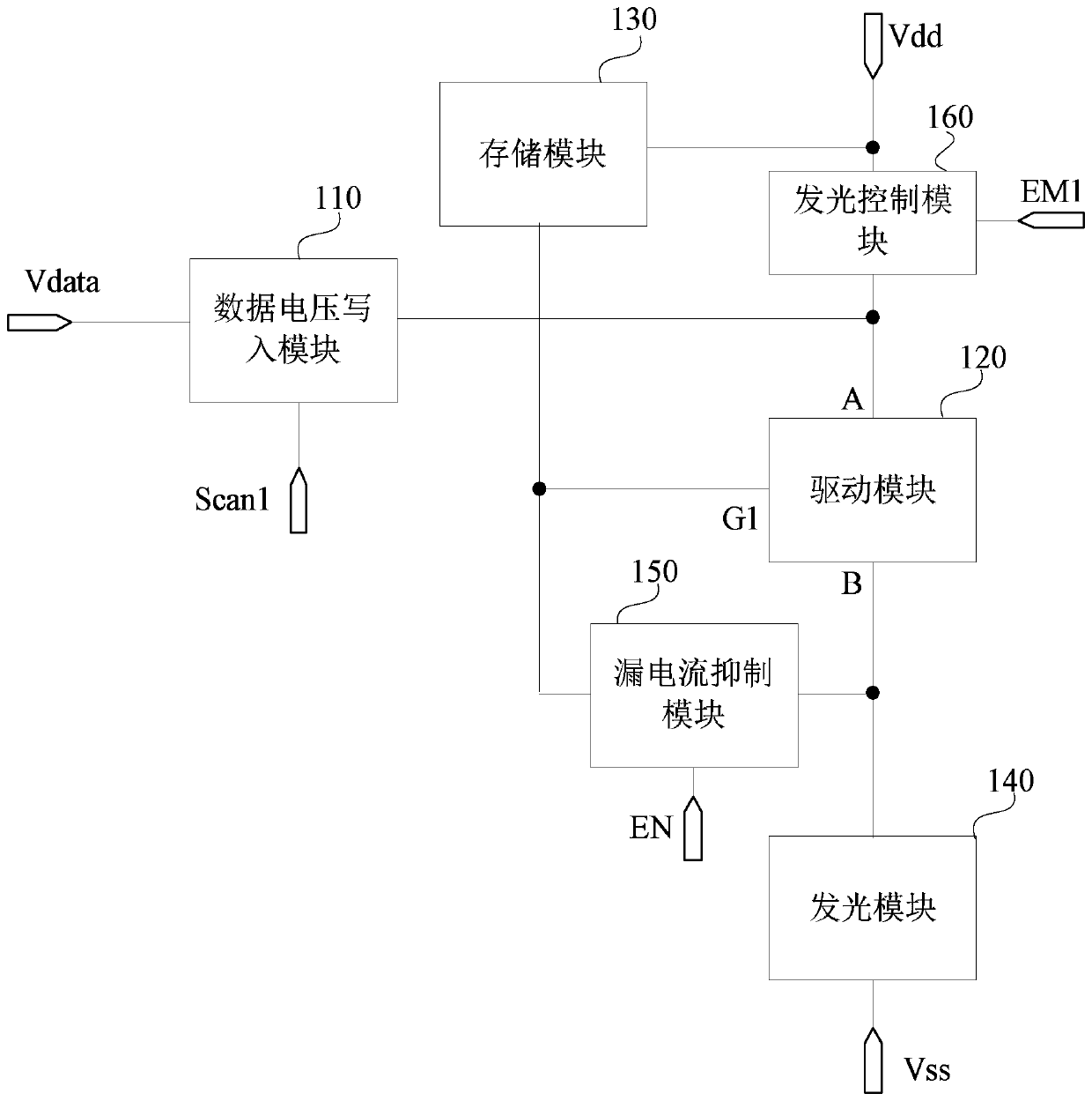
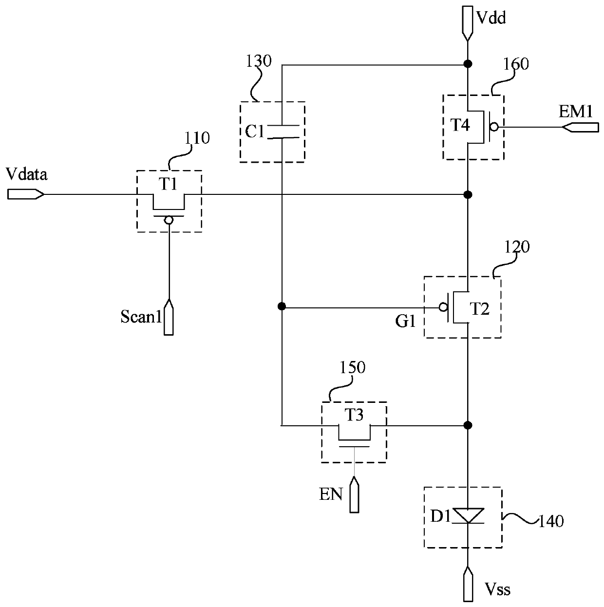
[0049] The present invention will be further described in detail below in conjunction with the accompanying drawings and embodiments. It should be understood that the specific embodiments described here are only used to explain the present invention, but not to limit the present invention. In addition, it should be noted that, for the convenience of description, only some structures related to the present invention are shown in the drawings but not all structures.

[0050] As mentioned in the background art, in the pixel circuit of the prior art, the thin film transistor electrically connected to the driving transistor usually has a large leakage current, which causes the gate potential of the driving transistor to be unstable, and the power consumption of the display device is large. The inventors found that the reason for the above problems is that in the prior art, the display device usually includes an array substrate, and the array substrate includes a thin film transisto...


PUM


Abstract

The embodiment of the invention discloses a pixel circuit and a display device. The pixel circuit comprises a data voltage write-in module, a driving module, a storage module, a light emitting module and a leakage current suppression module. The data voltage write-in module is used for writing data voltage into the control end of the driving module. The storage module is used for storing data voltage of the control end of the driving module. The driving module is used for driving the light-emitting module to emit light according to the data voltage of the control end of the driving module. The leakage current suppression module is electrically connected with the control end of the driving module and is used for maintaining the potential of the control end of the driving module. The potential of the control end of the driving module is not easy to release in the light emitting stage, so that the potential of the control end of the driving module can be well maintained, and the display effect is improved. Moreover, the driving frequency of the pixel circuit can be reduced, and the power consumption of the whole display device comprising the pixel circuit is reduced. And the area of the storage module can be reduced, so that the pixel density can be improved.

Description

technical field [0001] Embodiments of the present invention relate to the field of display technology, and in particular, to a pixel circuit and a display device. Background technique [0002] With the development of display technology, organic light-emitting display devices are more and more widely used. [0003] An organic light-emitting display device includes a plurality of pixel circuits, and the pixel circuit usually includes a plurality of thin film transistors. In the prior art, the thin film transistors in the pixel circuit are usually formed by a low temperature polysilicon (Low Temperature Poly-silicon, LTPS) process, and the LTPS process is used The leakage current of the formed thin film transistor is large, and the gate potential of the driving transistor is unstable, resulting in large power consumption of the display device. Contents of the invention [0004] The invention provides a pixel circuit and a display device to stabilize the potential of a contro...

Claims


Application Information

Patent Timeline
Patent Type & Authority Applications(China)
IPC IPC(8): G09G3/3225
CPCG09G3/3225G09G3/3233
Inventor 范龙飞文国哲朱晖
Owner HEFEI VISIONOX TECH CO LTD
Why Eureka
Try Eureka