Supercharge Your Innovation With Domain-Expert AI Agents!

Light emitting device, light emitting device package, and lighting apparatus including the package

A technology for light-emitting devices and devices, which is applied in the direction of electric solid-state devices, semiconductor devices, electrical components, etc., can solve the problems of reduced reliability, low adhesion, and easy peeling of light-emitting devices.

Active Publication Date: 2016-04-27
SUZHOU LEKIN SEMICON CO LTD
View PDF3 Cites 2 Cited by
  • Summary
  • Abstract
  • Description
  • Claims
  • Application Information

AI Technical Summary

Problems solved by technology

At this time, the reflective layer formed of a reflective material such as silver (Ag) has low adhesion to other layers and thus is easily peeled off, which may degrade the reliability of the light emitting device.

Method used


Image

  • Light emitting device, light emitting device package, and lighting apparatus including the package
  • Light emitting device, light emitting device package, and lighting apparatus including the package
  • Light emitting device, light emitting device package, and lighting apparatus including the package

Examples


Embodiment Construction

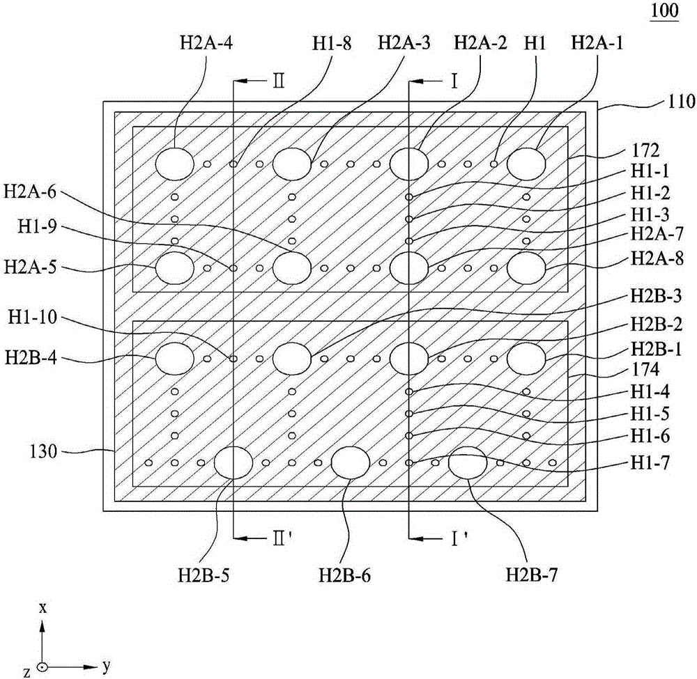
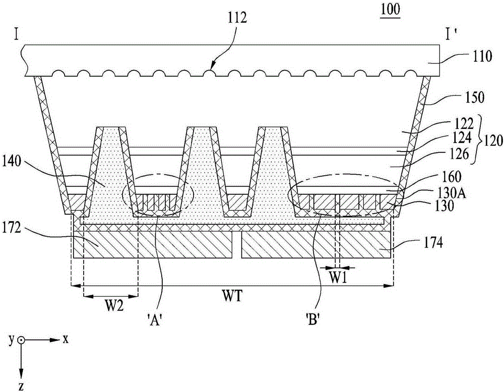
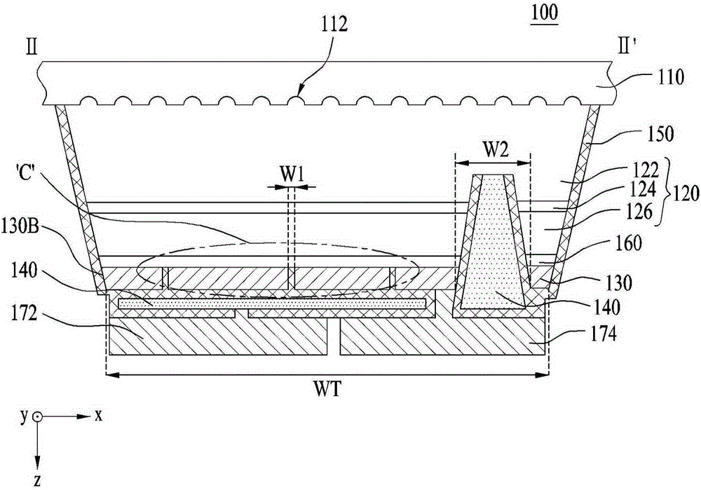
[0035] Hereinafter, exemplary embodiments will be described in detail with reference to the accompanying drawings to help understanding of the embodiments. However, the embodiment can be changed in various ways, and the scope of the embodiment should not be construed as being limited to the following description. These examples are intended to provide a more complete description to those skilled in the art.

[0036] In the following description of these embodiments, it will be understood that when each element is referred to as being formed "on" or "under" another element, it may be directly located "on" or "under" the other element. ", or one or more intermediate elements are indirectly formed between them. Additionally, it will also be understood that being "on" or "under" an element may mean both an upward orientation and a downward orientation of the element.

[0037] In addition, relative terms "first", "second", "top / upper / above", "bottom / under / under" and the like may ...


PUM


Abstract

Embodiments provide a light emitting device including a substrate, a light emitting structure including a first conductive semiconductor layer, an active layer, and a second conductive semiconductor layer, disposed under the substrate, a reflective layer disposed under the second conductive semiconductor layer, the reflective layer having at least one first through-hole formed in a first direction, the first direction being a thickness direction of the light emitting structure, a contact layer embedded in at least one second through-hole penetrating the reflective layer, the second conductive semiconductor layer, and the active layer so as to be connected to the first conductive semiconductor layer, and an insulation layer disposed between the contact layer and each of the reflective layer, the second conductive semiconductor layer, and the active layer, the insulation layer being embedded in the first through-hole.

Description

technical field [0001] Embodiments of the present disclosure relate to a light emitting device, a light emitting device package, and a lighting device including the package. Background technique [0002] A light emitting diode (LED) is a semiconductor device that converts electricity into light using properties of compound semiconductors to enable transmission / reception of signals, or it is used as a light source. [0003] Due to their physical and chemical properties, group III-V nitride semiconductors are attracting attention as core materials for light emitting devices such as LEDs or laser diodes (LDs). [0004] LEDs do not contain environmentally harmful substances such as mercury (Hg) used in conventional lighting equipment such as fluorescent lamps and incandescent bulbs, and are therefore very environmentally friendly and have several advantages such as long life and low power consumption. Therefore, traditional light sources are being rapidly replaced by LEDs. [...

Claims


Application Information

Patent Timeline
Patent Type & Authority Applications(China)
IPC IPC(8): H01L33/44H01L33/46H01L33/38
CPCH01L33/382H01L33/44H01L33/46H01L33/38H01L33/405H01L33/42H01L33/486H01L33/54H01L2224/16245H01L33/387H01L33/62
Inventor 李尚烈徐在元
Owner SUZHOU LEKIN SEMICON CO LTD
Features
  • R&D
  • Intellectual Property
  • Life Sciences
  • Materials
  • Tech Scout
  • Unparalleled Data Quality
  • Higher Quality Content
  • 60% Fewer Hallucinations
Learn More