An Optimization Method for Optical Proximity Correction Model

A technology for optical proximity correction and optimization methods, which is applied in optics, originals for opto-mechanical processing, and photoengraving processes for patterned surfaces, and can solve problems such as manufacturing technology failures and distortions.

Active Publication Date: 2019-12-17
SEMICON MFG INT (SHANGHAI) CORP
View PDF4 Cites 0 Cited by
  • Summary
  • Abstract
  • Description
  • Claims
  • Application Information

AI Technical Summary

Problems solved by technology

However, due to the shrinking of the size of semiconductor devices, distortion occurs in the process of transferring the pattern to the silicon wafer, resulting in optical proximity effect. If this distortion is not eliminated, it will lead to the failure of the entire manufacturing technology.

Method used


Image

  • An Optimization Method for Optical Proximity Correction Model
  • An Optimization Method for Optical Proximity Correction Model
  • An Optimization Method for Optical Proximity Correction Model

Examples


Embodiment 1

[0049] The method of the present invention will be described in further detail below through an embodiment of the present invention.

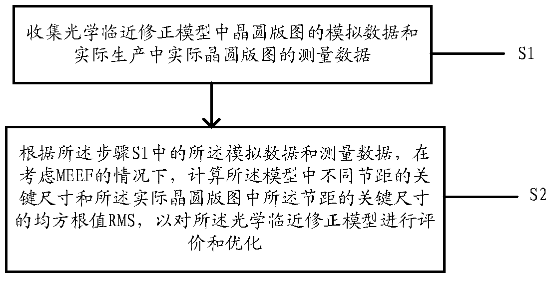
[0050] The method described in this embodiment comprises the following steps:

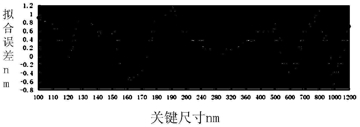
[0051] (1) Carry out the actual production of the wafer, obtain the physical wafer, measure the key dimensions of the corresponding features in the simulation process, and obtain the CD i(测量) ;

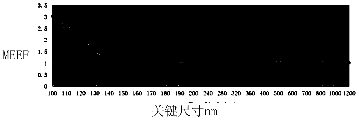
[0052] (2) Measure the value of MEEF in the physical wafer to obtain MEEF i ;

[0053] (3) Establish an OPC model according to the target pattern and the measurement results on the actual wafer, select the OPC model for simulation, and measure the key dimensions of different features to obtain CD i(模拟) ;

[0054] (4) select formula 1 to evaluate described simulation result, so that described simulation structure is detected, make OPC final result more reasonable;

[0055]

[0056] Specifically, in step (1), the actual production of the wafer is first carried out to ...


PUM


Abstract

The invention provides an optimization method for an OPC model. The optimization method comprises the following steps: step 1, collecting simulated data of a wafer layout in the OPC model and measured data of an actual wafer layout in actual production; and step 2, according to the simulated data and the measured data collected in the step 1, calculating critical dimensions of different pitches in the model and the root-mean-square value (RMS) of critical dimensions of the pitches in the actual wafer layout according to a formula (I) described in the specification so as to evaluate and optimize the OPC model. In the formula (I), Wi is the weight of the critical dimensions of the pitches; CDi<simulated> is the simulated value of the critical dimensions of different pitches in the model; CDi<measured> is the measured value of the critical dimensions of the pitches in the actual wafer layout; and MEEFi is a mask error enhancement factor of the pitches. The optimization method has the advantage that final OPC results are ensured to be more reasonable and more accurate.

Description

technical field [0001] The invention relates to the field of semiconductors, and in particular, the invention relates to an optimization method of an optical proximity correction model. Background technique [0002] Integrated circuit manufacturing technology is a complicated process, and the technology is updated very quickly. A key parameter that characterizes the integrated circuit manufacturing technology is the minimum feature size, that is, the critical dimension (CD). With the continuous development of technology, the critical dimension is continuously reduced. It is precisely because of the reduction of the critical dimension that the settings on each chip Millions of devices are possible. [0003] Photolithography is the driving force behind the development of integrated circuit manufacturing processes, and it is also one of the most complex technologies. Compared with other single manufacturing technologies, the improvement of lithography technology is of great s...

Claims


Application Information

Patent Timeline
Patent Type & Authority Patents(China)
IPC IPC(8): G03F1/36
Inventor 舒强王铁柱
Owner SEMICON MFG INT (SHANGHAI) CORP
Why Eureka
Try Eureka