Electronic product case and manufacturing method thereof

A technology of electronic products and manufacturing methods, which is applied in the direction of electrical equipment casings/cabinets/drawers, electrical components, metal casings, etc., and can solve problems that affect product durability and poor surface protection effects

Active Publication Date: 2016-05-11
GUANGDONG OPPO MOBILE TELECOMM CORP LTD
View PDF10 Cites 40 Cited by
  • Summary
  • Abstract
  • Description
  • Claims
  • Application Information

AI Technical Summary

Problems solved by technology

However, the traditional fashion electronic product shell has poor prote...

Method used


Image

  • Electronic product case and manufacturing method thereof
  • Electronic product case and manufacturing method thereof

Examples


Embodiment 1

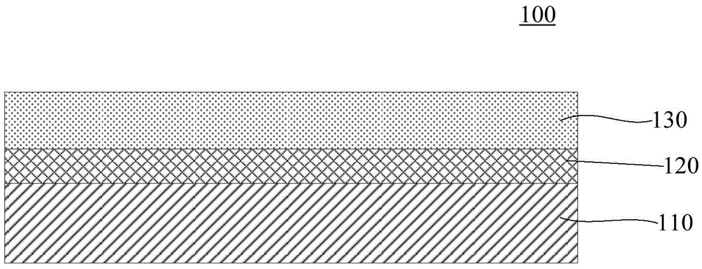
[0032] Please refer to figure 1 , the electronic product casing 100 of the first embodiment includes an aluminum alloy main body layer 110 , an anodized layer 120 and a flash point effect layer 130 . Wherein, the anodized layer 120 is disposed on the aluminum alloy body layer 110 . The flash point effect layer 130 is provided on the anodized layer 120 . The flash point effect layer 130 can make the housing 100 of the electronic product have a flash point effect, which is beneficial to improve the appearance effect of the product and enhance user experience.

[0033] In this embodiment, the flash point effect layer 130 is a paint layer doped with flash particles. The flash point effect layer 130 may be one or more layers. When the flash point effect layer 130 is multi-layered, the multi-layer flash point effect layers 130 may be stacked.

[0034] The thickness of the flash point effect layer 130 in this embodiment is 5 μm-30 μm. Wherein, the particle size of the glitter pa...

Embodiment 2

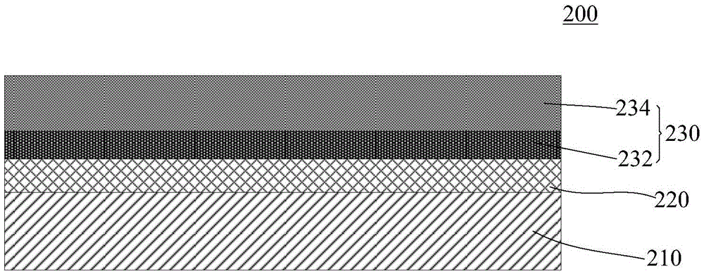
[0055] Please refer to figure 2 , the electronic product case 200 of the second embodiment includes an aluminum alloy main body layer 210 , an anodized layer 220 and a flash point effect layer 230 . Wherein, the anodized layer 220 is disposed on the aluminum alloy body layer 210 . The flash point effect layer 230 is disposed on the anodized layer 220 . The flash point effect layer 230 can make the housing 200 of the electronic product have a flash point effect, which is beneficial to improve the appearance effect of the product and enhance user experience.

[0056] In this embodiment, the flash point effect layer 230 includes a flash particle layer 232 and a paint layer 234 . Both the glitter particle layer 232 and the paint layer 234 can be one or more layers, and the number of the glitter particle layer 232 is the same as that of the paint layer 234 . When both the glitter particle layer 232 and the paint layer 234 have multiple layers, the multiple layers of glitter par...


PUM

PropertyMeasurementUnit
Thicknessaaaaaaaaaa
Thicknessaaaaaaaaaa
Particle sizeaaaaaaaaaa

Abstract

The invention relates to an electronic product case and a manufacturing method thereof. The electronic product case comprises a metal or alloy body layer and a flashing effect layer arranged on the metal or alloy body layer. The flashing effect layer is a coating layer doped with flashing particles, or the flashing effect layer is an overlaying structure formed by a flashing particle layer and the coating layer that is outside, or the flashing effect layer is a mixed layer overlaid by the coating layer doped with flashing particles and the overlaying structure. The electronic product case has a flashing effect, can make the product more fashionable, and improves the user experience. According to the manufacturing method, the coating layer is sprayed and prepared on the metal or alloy case material, so that the appearance of the product is effectively protected and is less likely to wear.

Description

technical field [0001] The invention relates to the field of electronic product casings, in particular to an electronic product casing and a manufacturing method thereof. Background technique [0002] As electronic products, especially hand-held electronic terminal products, are more and more widely used, users have higher and higher requirements for electronic product casings. Novel, fashionable and cool electronic product casings have become the common choice of many consumers. However, the traditional fashion electronic product shell has poor protection effect on the surface layer, which affects the durability of the product. Contents of the invention [0003] Based on this, it is necessary to provide an electronic product casing capable of forming effective protection on the surface and a manufacturing method thereof. [0004] An electronic product casing, comprising a metal or alloy main body layer and a flash point effect layer arranged on the metal or alloy main b...

Claims


Application Information

Patent Timeline
IPC IPC(8): H05K5/04H05K5/02
CPCH05K5/0243H05K5/04
Inventor 刘孟帅罗元礼朱士强刘永菁
Owner GUANGDONG OPPO MOBILE TELECOMM CORP LTD
Why Eureka
Try Eureka