Low resistance contacts including intermetallic alloy of nickel, platinum, titanium, aluminum and type iv semiconductor elements

a technology of contact and low resistance, applied in the direction of semiconductor devices, electrical apparatus, semiconductor/solid-state device details, etc., can solve problems affecting the performance and reliability of fabricated circuits

Active Publication Date: 2018-03-08
IBM CORP
View PDF6 Cites 252 Cited by
  • Summary
  • Abstract
  • Description
  • Claims
  • Application Information

AI Technical Summary

Problems solved by technology

The quality of the interconnection structure drastically affects the performance and reliability of the fabricated circuit.

Method used


Image

  • Low resistance contacts including intermetallic alloy of nickel, platinum, titanium, aluminum and type iv semiconductor elements
  • Low resistance contacts including intermetallic alloy of nickel, platinum, titanium, aluminum and type iv semiconductor elements
  • Low resistance contacts including intermetallic alloy of nickel, platinum, titanium, aluminum and type iv semiconductor elements

Examples


Embodiment Construction

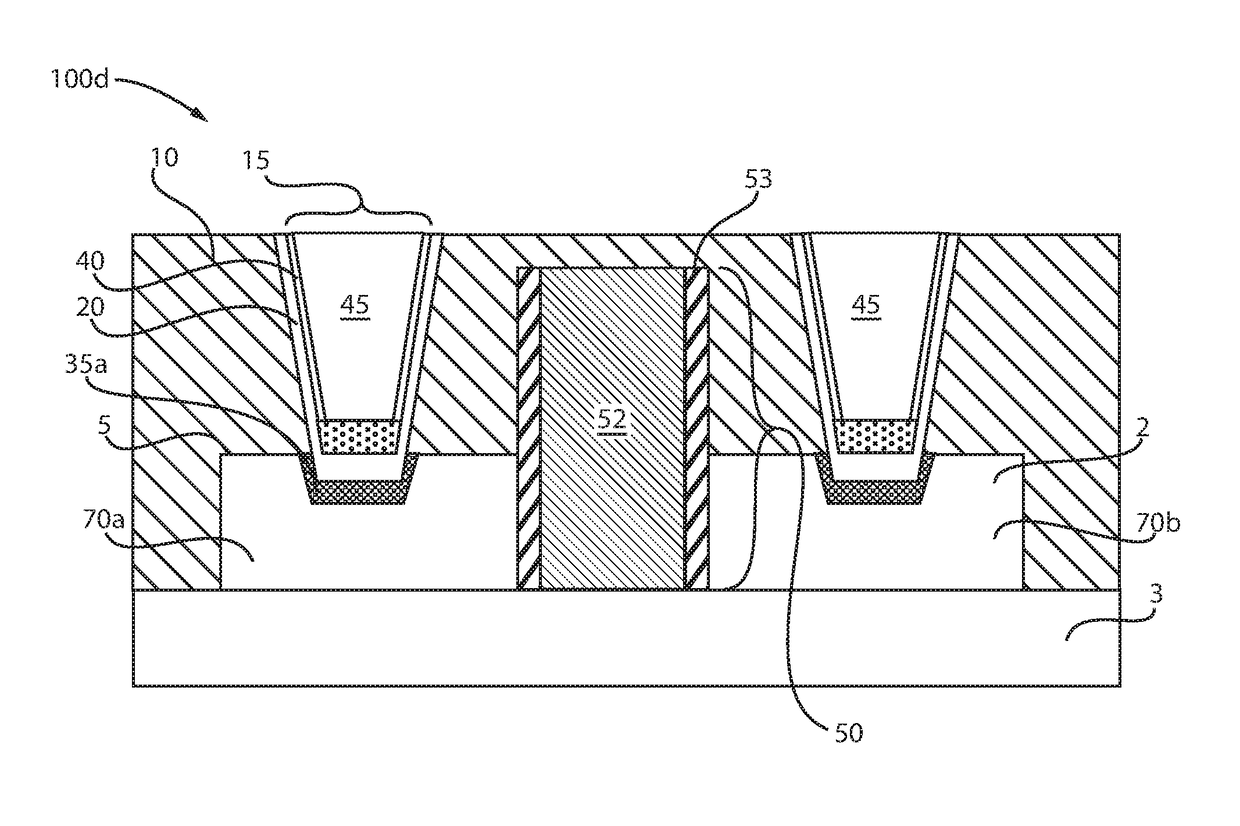
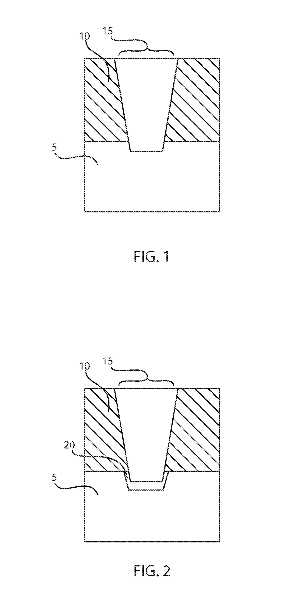
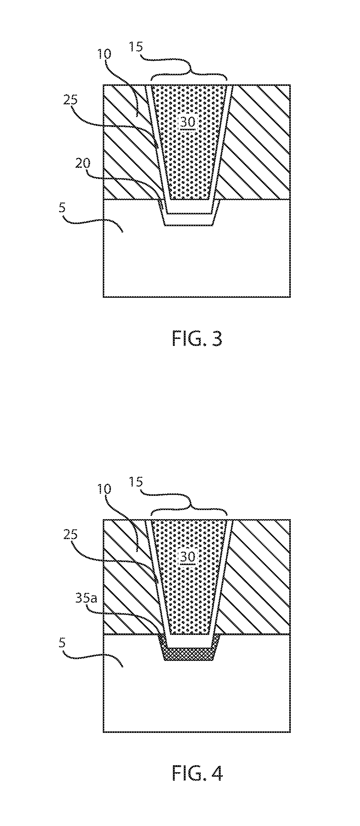
[0017]Detailed embodiments of the claimed structures and methods are described herein; however, it is to be understood that the described embodiments are merely illustrative of the claimed structures and methods that may be embodied in various forms. In addition, each of the examples given in connection with the various embodiments are intended to be illustrative, and not restrictive. Further, the figures are not necessarily to scale, some features may be exaggerated to show details of particular components. Therefore, specific structural and functional details described herein are not to be interpreted as limiting, but merely as a representative basis for teaching one skilled in the art to variously employ the methods and structures of the present description. For purposes of the description hereinafter, the terms “upper”, “lower”, “right”, “left”, “vertical”, “horizontal”, “top”, “bottom”, and derivatives thereof shall relate to the embodiments of the described methods and structu...


PUM

PropertyMeasurementUnit
temperatureaaaaaaaaaa
thicknessaaaaaaaaaa

Abstract

A method of forming a contact to a semiconductor device is provided that forms an alloy composed of nickel (Ni), platinum (Pt), aluminum (Al), titanium (Ti) and a semiconductor material. The methods may include forming a nickel and platinum semiconductor alloy at a base of a via. A titanium layer having an angstrom scale thickness is deposited in the via in contact with the nickel platinum semiconductor alloy. An aluminum containing fill is deposited atop the titanium layer. A forming gas anneal including an oxygen containing atmosphere is applied to the structure to provide a contact alloy comprising nickel, platinum, aluminum, titanium and a semiconductor element from the contact surface of the semiconductor device.

Description

BACKGROUNDTechnical Field[0001]The methods and structures described herein relate to contact structures and structures for transmitting electrical current.Description of the Related Art[0002]Modern integrated circuits are made up of literally millions of active devices such as transistors and capacitors. These devices are initially isolated from one another but are later interconnected together to formed functional circuits. The quality of the interconnection structure drastically affects the performance and reliability of the fabricated circuit. Interconnects and contacts are typically formed to bring and transmit electrical signals to semiconductor devices.SUMMARY[0003]In one embodiment, a method of forming a contact to a semiconductor device is provided that forms an alloy composed of nickel (Ni), platinum (Pt), aluminum (Al), titanium (Ti) and a semiconductor material, such as silicon (Si). In one embodiment, the methods includes forming a nickel and platinum semiconductor alloy...

Claims


Application Information

Patent Timeline
Patent Type & Authority Applications(United States)
IPC IPC(8): H01L23/535H01L23/532H01L29/78H01L21/768C22C30/00
CPCH01L23/535H01L23/53266H01L29/7851C22C30/00H01L21/76846H01L21/76864H01L21/76895H01L21/76805H01L23/485H01L23/53209H01L23/53223H01L23/53238H01L23/53252H01L21/28518H01L21/2855H01L21/76843H01L21/76858
Inventor BRULEY, JOHNCHU, JACK O.LEE, KAM-LEUNGOZCAN, AHMET S.SOLOMON, PAUL M.YAU, JENG-BANG
Owner IBM CORP
Why Eureka
Try Eureka