Display substrate, display device and manufacturing method of display device

A technology for display devices and substrates, which is used in semiconductor/solid-state device manufacturing, instruments, nonlinear optics, etc., can solve the problems of impure colors and limited luminous efficiency of color filter layers, and achieves improved display color gamut, improved Luminous efficiency and utilization, the effect of reducing power consumption

Active Publication Date: 2016-05-25
BOE TECH GRP CO LTD +1
View PDF4 Cites 27 Cited by
  • Summary
  • Abstract
  • Description
  • Claims
  • Application Information

AI Technical Summary

Problems solved by technology

Because the material of the color filter layer itself includes small dye molecules, which will absorb part of the light emitted by the backlight module, the luminous efficiency of the color filter layer is limited; in addition, the backlight module usually uses LED (light emitting diode) as the light source, and the LED emits light. The half-maximum width of the light is wide and the color of the light formed by the interaction with the material of the color filter layer is impure

Method used


Image

  • Display substrate, display device and manufacturing method of display device
  • Display substrate, display device and manufacturing method of display device
  • Display substrate, display device and manufacturing method of display device

Examples


Embodiment Construction

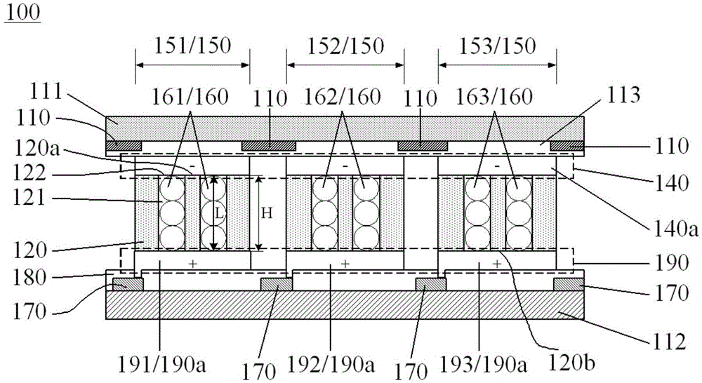
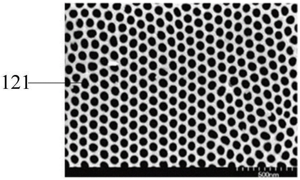
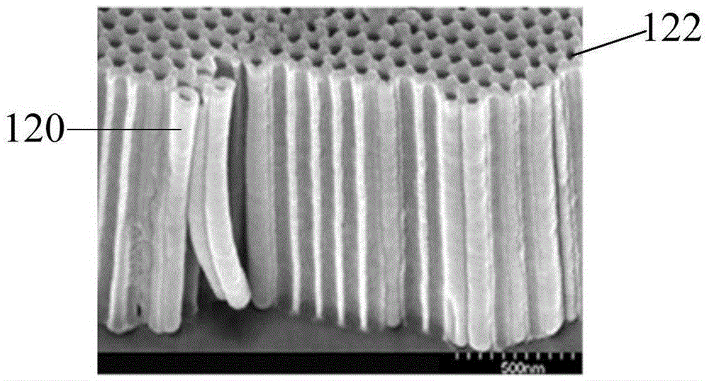
[0040] In order to make the purpose, technical solutions and advantages of the embodiments of the present disclosure clearer, the technical solutions of the embodiments of the present disclosure will be clearly and completely described below in conjunction with the accompanying drawings of the embodiments of the present disclosure. Apparently, the described embodiments are some of the embodiments of the present disclosure, not all of them. Based on the described embodiments of the present disclosure, all other embodiments obtained by persons of ordinary skill in the art without creative effort fall within the protection scope of the present disclosure.

[0041]Unless otherwise defined, the technical terms or scientific terms used in the present disclosure shall have the usual meanings understood by those skilled in the art to which the present disclosure belongs. "First", "second" and similar words used in the present disclosure do not indicate any order, quantity or importanc...


PUM

PropertyMeasurementUnit
sizeaaaaaaaaaa
sizeaaaaaaaaaa
thicknessaaaaaaaaaa

Abstract

The invention provides a display substrate, a display device and a manufacturing method of the display device. The display device comprises an ordered porous film, a plurality of quantum dots, first electrode layers and second electrode layers, wherein the ordered porous film comprises sub-pixel areas which are arranged in a matrix; a plurality of ducts are arranged in each sub-pixel area; the extension direction of each duct and the surface of the ordered porous film form an angle which is not zero; each duct is provided with an opening in the surface of the ordered porous film; the plurality of quantum dots are arranged in at least partial ducts respectively; the first electrode layers and the second electrode layers are arranged at two sides of the ordered porous film respectively; each second electrode layer comprises a plurality of sub-electrodes which are arranged at intervals; and the sub-electrodes correspond to the sub-pixel areas respectively. The display substrate, the display device and the manufacturing method of the display device have relatively high color ranges and quantum-dot luminous efficiency.

Description

technical field [0001] Embodiments of the present disclosure relate to a display substrate, a display device and a manufacturing method thereof. Background technique [0002] A liquid crystal display usually utilizes a color filter layer included in it to filter, for example, white light emitted by a backlight module to form light of different colors through light mixing, thereby realizing color display. Because the material of the color filter layer itself includes small dye molecules, which will absorb part of the light emitted by the backlight module, the luminous efficiency of the color filter layer is limited; in addition, the backlight module usually uses LED (light-emitting diode) as the light source, and the LED emits The half peak width of the light is wide and the color of the light formed by the interaction with the material of the color filter layer is impure. [0003] As a new type of semiconductor nanomaterial, quantum dots have many unique nano-properties. I...

Claims


Application Information

Patent Timeline
Patent Type & Authority Applications(China)
IPC IPC(8): H01L27/32H01L51/50
CPCH10K59/12H10K50/115G02F2202/36G02F1/133514G02F1/133602G02F1/1343G02F1/13454G02F1/136209
Inventor 江亮亮王海峰郭磊
Owner BOE TECH GRP CO LTD
Why Eureka
Try Eureka