OLED display device and manufacturing method thereof, color filter substrate and manufacturing method thereof

A technology of a display device and a manufacturing method, which is applied to chemical instruments and methods, semiconductor/solid-state device manufacturing, instruments, etc., can solve the problems of low display brightness of OLED display devices, increased cost of OLED display devices, and expensive quantum dot materials, etc. , to achieve the effect of low price, improved stability and high luminous brightness

Active Publication Date: 2017-03-08
BOE TECH GRP CO LTD
View PDF3 Cites 0 Cited by
  • Summary
  • Abstract
  • Description
  • Claims
  • Application Information

AI Technical Summary

Problems solved by technology

[0004] However, since monochromatic light is obtained by color-resistive filtering, the light transmittance of the above-mentioned color filter layer is low, resulting in low display brightness of the OLED display device.
Although there is currently a method of increasing the color resistance of W (white) color in the color filter layer to improve the display brightness, increasing the color resistance of W (white) color in the color filter layer will cause the reduction of the display color gamut. Small; in addition, there is also the use of quantum dots to form a color film layer, so that the light-emitting structure layer that can emit blue light or ultraviolet light emits light to stimulate the quantum dots in the color film layer to emit RGB monochromatic light. Although this method can improve display brightness , and increase the display color gamut, but the quantum dot material is expensive and easy to oxidize, resulting in an increase in the cost of the OLED display device, and the display stability is not high

Method used


Image

  • OLED display device and manufacturing method thereof, color filter substrate and manufacturing method thereof
  • OLED display device and manufacturing method thereof, color filter substrate and manufacturing method thereof
  • OLED display device and manufacturing method thereof, color filter substrate and manufacturing method thereof

Examples


Embodiment 1

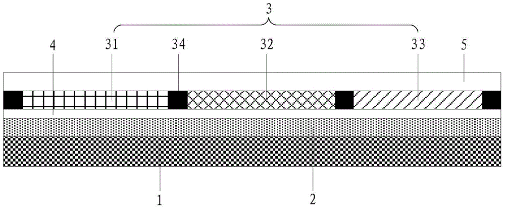
[0038] This embodiment provides an OLED display device, such as figure 1 As shown, the OLED display device includes: a TFT array substrate 1; a light emitting structure layer 2 disposed on the TFT array substrate 1, the light emitted by the light emitting structure layer 2 is infrared light; a light conversion layer located on the light emitting structure layer 2 3. The light conversion layer 3 includes a plurality of pixel areas, and each pixel area is provided with at least three light conversion units of red light, green light and blue light.

[0039] Among them, the red light conversion unit 31 is formed by an up-conversion luminescent material that emits red light after being excited by infrared light; the green light conversion unit 32 is formed by an up-conversion luminescent material that emits green light after being excited by infrared light; the blue light conversion unit 33 is formed by an up-conversion luminescent material that emits blue light after being excited...

Embodiment 2

[0051] This embodiment provides a method for manufacturing an OLED display device, the method comprising the following steps:

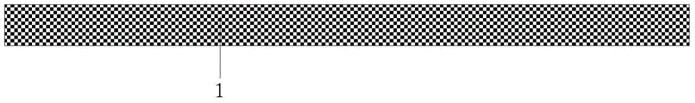
[0052] Step S1: if Figure 3a As shown, a TFT array substrate 1 was fabricated.

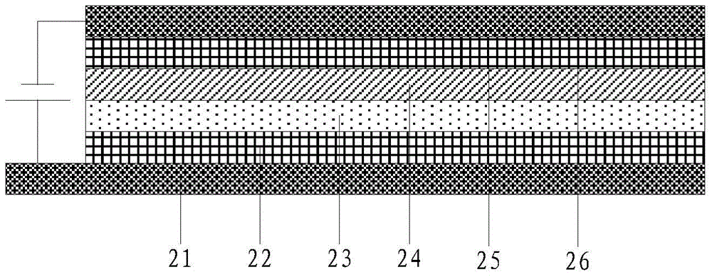
[0053] Step S2: if Figure 3b As shown, a light emitting structure layer 2 is formed on a TFT array substrate 1, and the light emitted by the light emitting structure layer 2 is infrared light.

[0054] Step S3: forming a light conversion layer, the light conversion layer is located on the light-emitting structure layer, the light conversion layer includes a plurality of pixel areas, and at least three light conversion units of red light, green light and blue light are arranged in each pixel area. Among them, the red light conversion unit is formed by an up-conversion luminescent material that emits red light after being excited by infrared light; the green light conversion unit is formed by an up-conversion luminescent material that emits green light after being excit...

Embodiment 3

[0067] This embodiment provides a color filter substrate, such as Figure 3e As shown, the color filter substrate includes: a base substrate 5; a light conversion layer 3 disposed on the base substrate 5, the light conversion layer 3 includes a plurality of pixel regions, each pixel region is provided with at least red light, green Three light conversion units for light and blue light. Among them, the red light conversion unit 31 is formed by an up-conversion luminescent material that emits red light after being excited by infrared light; the green light conversion unit 32 is formed by an up-conversion luminescent material that emits green light after being excited by infrared light; the blue light conversion unit 33 is formed by an up-conversion luminescent material that emits blue light after being excited by infrared light.

[0068] In the above-mentioned color filter substrate, different up-conversion light-emitting materials are used to form red light, green light and bl...


PUM


Abstract

The invention provides an OLED display device and a manufacturing method thereof, a color filter substrate and a manufacturing method thereof, and relates to the field of display technology, which can improve the display brightness of the display device and increase the display color gamut. Wherein the OLED display device includes: a TFT array substrate, a light-emitting structure layer arranged on the TFT array substrate, the light emitted by the light-emitting structure layer is infrared light; a light conversion layer located on the light-emitting structure layer, the light conversion layer includes A plurality of pixel areas, each pixel area is provided with at least three light conversion units of red light, green light and blue light; the red light conversion unit is formed by an up-conversion luminescent material that emits red light after being excited by infrared light; The conversion unit is formed by an up-conversion luminescent material that emits green light after being excited by infrared light; the blue light conversion unit is formed by an up-conversion luminescent material that emits blue light after being excited by infrared light. The OLED display device described above is used to display images.

Description

technical field [0001] The present invention relates to the field of display technology, in particular to an OLED (Organic Light-Emitting Diode, Organic Light-Emitting Diode) display device and a manufacturing method thereof, a color filter substrate and a manufacturing method thereof. Background technique [0002] OLED display device is an active light-emitting display device, which has excellent characteristics such as high contrast, thin thickness, wide viewing angle, fast response speed, can be used for flexible panels, wide operating temperature range, simple structure and manufacturing process, etc., and is widely used. In mobile phones, PDA (Personal Digital Assistant, personal digital assistant), notebook computers, digital video cameras, DVD (Digital Versatile Disc, Digital Versatile Disc) machines, car audio and television and other fields. [0003] The structure of a traditional OLED display device mainly includes: a TFT (Thin Film Transistor, thin film transistor...

Claims


Application Information

Patent Timeline
Patent Type & Authority Patents(China)
IPC IPC(8): H01L27/32H01L51/52
CPCH10K59/122H10K50/865C09K11/7773G02B5/201G02B1/14H10K59/38H10K50/11H10K2102/331
Inventor 李颖祎
Owner BOE TECH GRP CO LTD
Why Eureka
Try Eureka