Organic light emitting display device and fabricating method using the same

A light-emitting display and organic technology, applied in semiconductor/solid-state device manufacturing, instruments, electric solid-state devices, etc., can solve the problems of reducing sensing characteristics, reducing the overall sensitivity of the touch panel, etc., and achieve the effect of reducing surface reflection

Active Publication Date: 2016-06-01
LG DISPLAY CO LTD
View PDF5 Cites 16 Cited by
  • Summary
  • Abstract
  • Description
  • Claims
  • Application Information

AI Technical Summary

Problems solved by technology

However, the distance between the electrode 26 and the touch electrode 52 also decreases (d1→d2) at the same time, so the parasitic capacitance component formed between the electrode 26 and the touch electrode 52 increases (c1→c2)
The parasitic capacitive component (c2) may have an effect on the touch electrodes 52 to reduce the sensing characteristics, thereby reducing the overall sensitivity of the touch panel
[0014] As a result, a distance (d1) higher than a predetermined level should be maintained between the electrodes 26 on the lower substrate 10 and the touch electrodes 52, resulting in limitations in widening the viewing angle of the display device.

Method used


Image

  • Organic light emitting display device and fabricating method using the same
  • Organic light emitting display device and fabricating method using the same
  • Organic light emitting display device and fabricating method using the same

Examples


Embodiment Construction

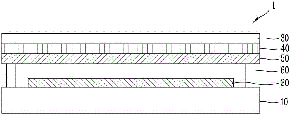
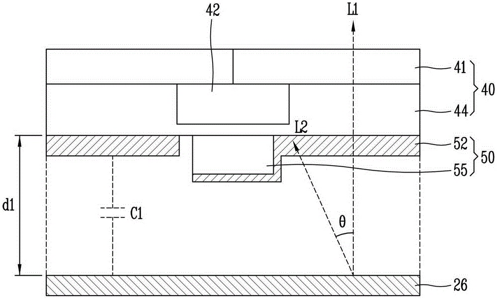
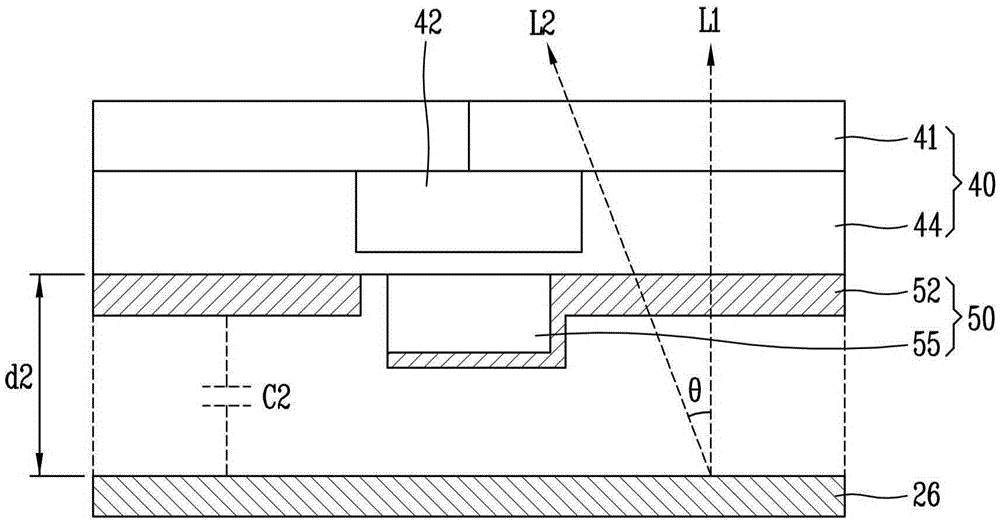
[0029] Advantages and features of the present disclosure and methods of achieving them will be clearly understood with reference to the following embodiments described in detail with reference to the accompanying drawings. However, the present disclosure is not limited to the embodiments disclosed below, but may be implemented in various forms. It should be noted that the present embodiments are only provided to fully disclose the present invention and thus also enable those skilled in the art to appreciate the full scope of the present invention.

[0030] The shapes, dimensions, ratios, angles, numbers, etc. disclosed in the drawings for describing the embodiments of the present disclosure may be illustrative, and thus may not necessarily be limited to the details illustrated in the present disclosure. Furthermore, the same reference numerals designate the same or similar elements throughout the specification. In describing the embodiments of the present disclosure, when spe...


PUM


Abstract

Provided are an organic light emitting display device and a fabricating method using the same. The organic light emitting display device (100) and a fabrication method comprising a touch electrode layer (150) including touch electrodes (152) and touch lines (155) on an upper substrate (130) which are directly formed on the upper substrate (130) to secure a large distance between the touch electrodes (152) and cathode as well as minimize a distance between the upper and lower substrates (110, 130), thereby widening the viewing angle of an image while reducing a parasitic capacitance.

Description

technical field [0001] The present disclosure relates to an organic light emitting display device, and more particularly, to an organic light emitting display device of an in-cell type touch integrated display device and a manufacturing method thereof. Background technique [0002] Display devices are used in electronic devices and the like. Touch screens have been implemented to enable users to select graphical objects or regions displayed on the touch screen. [0003] The touch screen for the display device can be implemented as an add-on type touch screen in which a touch panel is adhered to the display panel, or an in-cell type touch integrated display device in which touch electrodes and touch sensing lines are formed inside the display panel. . In particular, an in-cell type touch-integrated display device is advantageous due to its improved touch sensitivity and thin nature. [0004] The first substrate has a light-emitting unit, and the second substrate has a colo...

Claims


Application Information

Patent Timeline
Patent Type & Authority Applications(China)
IPC IPC(8): H01L27/32H01L51/52H01L51/56G06F3/044
CPCH10K59/38H10K59/40H10K59/1315H10K59/1201H10K50/86H10K50/856H10K71/00
Inventor 李副烈赵南旭金炯洙李在冕
Owner LG DISPLAY CO LTD
Why Eureka
Try Eureka