Printed circuit board and mobile terminal

A technology of printed circuit boards and substrates, applied in the direction of printed circuits, printed circuits, printed circuit components, etc., can solve the problems of electrostatic interference and inability to absorb static electricity of circuit components, and achieve the effect of preventing electrostatic interference and ensuring high-quality transmission

Active Publication Date: 2016-06-01
GUANGDONG OPPO MOBILE TELECOMM CORP LTD
View PDF3 Cites 6 Cited by
  • Summary
  • Abstract
  • Description
  • Claims
  • Application Information

AI Technical Summary

Problems solved by technology

[0003] People in the industry usually shield the static electricity by covering the two surfaces of the printed circuit board with a shielding film layer. However, the shielding fi

Method used


Image

  • Printed circuit board and mobile terminal
  • Printed circuit board and mobile terminal
  • Printed circuit board and mobile terminal

Examples


Embodiment Construction

[0024] The following will clearly and completely describe the technical solutions in the embodiments of the present invention with reference to the drawings in the embodiments of the present invention.

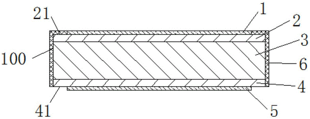
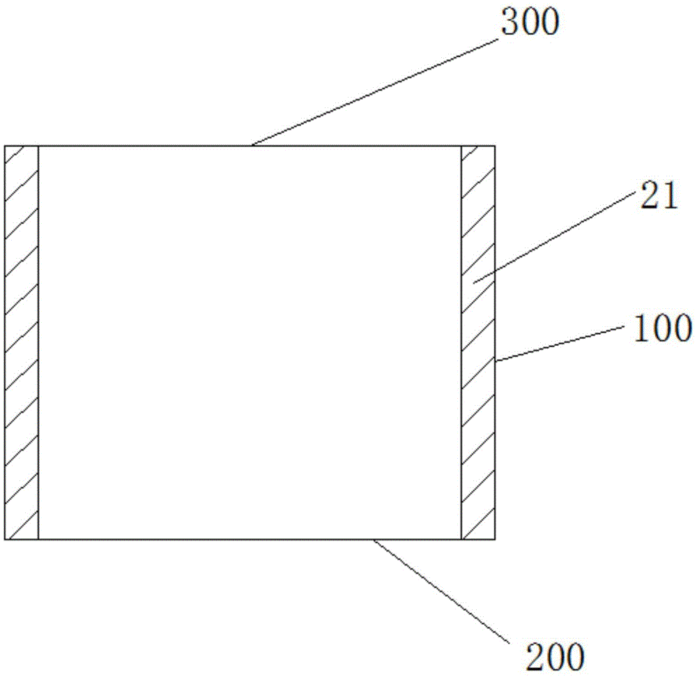
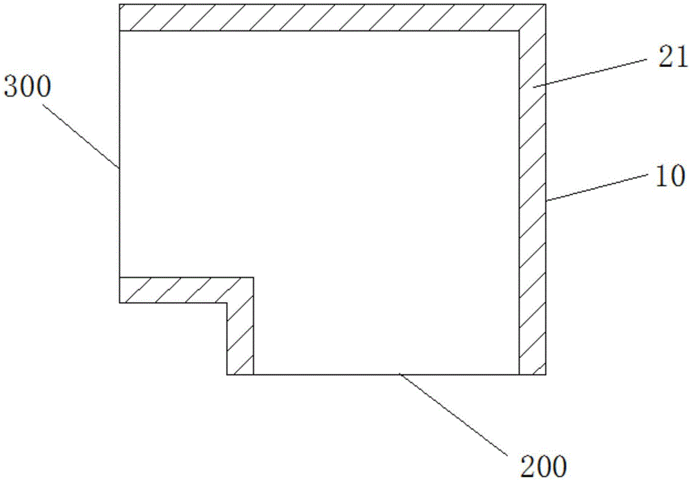
[0025] see figure 1 and figure 2 , figure 1 A schematic cross-sectional view of a printed circuit board provided by an embodiment of the present invention, figure 2 A schematic top view structural diagram of a printed circuit board not including a shield bracket provided for an embodiment of the present invention. like figure 1 As shown, the embodiment of the present invention provides a printed circuit board, including a first protective layer 1, a first shielding layer 2, a circuit layer 3, a second shielding layer 4 and a second protective layer 5, which are sequentially stacked. Layer 3 includes data signal wires and ground wires, and the ground wires are electrically connected to the first shielding layer 2 and the second shielding layer 4 . like figure 1 and fi...


PUM

PropertyMeasurementUnit
Sizeaaaaaaaaaa

Abstract

The invention discloses a printed circuit board. The printed circuit board comprises a first protection layer, a first shielding layer, a circuit layer, a second shielding layer and a second protection layer, which are successively laminated. The circuit layer comprises a data signal line and a grounding line. The grounding line is electrically connected with the first shielding layer and the second shielding layer. The peripheral side faces of the printed circuit board comprise an input face, an output face and a non connection face. A first shielding region which is not covered by the first protection layer is formed in a position near the non connection face of the first shielding layer. A second shielding region which is not covered by the second protection layer is formed in a position near the non connection face of the second shielding layer. The printed circuit board comprises a shielding support which is electrically connected with the first shielding region or/and the second shielding region and covers the non connection face. The printed circuit board is capable of preventing static interference. The invention also discloses a mobile terminal.

Description

technical field [0001] The invention relates to the field of printed circuit boards, in particular to a printed circuit board with antistatic function and a mobile terminal. Background technique [0002] Electrostatic discharge refers to the charge transfer caused by objects with different electrostatic potentials approaching each other or in direct contact. Electrostatic discharge can easily damage sensitive circuit components. Especially for printed circuit boards, the existing printed circuit boards often use a large number of integrated circuit components, which have high electrostatic sensitivity, low voltage resistance, and weak electrostatic shock resistance, so they are easily damaged by electrostatic discharge, and even further affect the The normal operation of the entire electronic device system. Therefore, it is necessary to protect the printed circuit board from static electricity and release the static electricity in time. [0003] People in the industry usu...

Claims


Application Information

Patent Timeline
IPC IPC(8): H05K1/02
CPCH05K1/0218H05K1/023H05K2201/0715H05K2201/10371
Inventor 黄占肯
Owner GUANGDONG OPPO MOBILE TELECOMM CORP LTD
Why Eureka
Try Eureka