
Array substrate and plane conversion liquid crystal display panel

A technology of array substrates and substrates, which is applied in the fields of instruments, nonlinear optics, and optics, and can solve problems such as too small viewing angles, crosstalk, and negative effects on display effects

Inactive Publication Date: 2016-06-08
AU OPTRONICS CORP
View PDF7 Cites 10 Cited by
  • Summary
  • Abstract
  • Description
  • Claims
  • Application Information

AI Technical Summary

Problems solved by technology

In order to solve the shortcoming of the existing liquid crystal display with too small viewing angle, the industry has developed an in-plane switching (IPS) liquid crystal display whose main feature is that both the common electrode and the pixel electrode are arranged on the array substrate, and by The horizontal electric field generated by the common electrode and the pixel electrode drives the arrangement of liquid crystal molecules, thereby achieving the effect of wide viewing angle
However, under the design premise of increasing the pixel aperture ratio as much as possible, the horizontal electric fields in adjacent pixel regions are likely to interact with each other, resulting in crosstalk, resulting in a negative impact on the display effect.

Method used


Image

  • Array substrate and plane conversion liquid crystal display panel
  • Array substrate and plane conversion liquid crystal display panel
  • Array substrate and plane conversion liquid crystal display panel

Examples


Embodiment Construction

[0045] In order to enable those who are familiar with the technical field of the present invention to further understand the present invention, the preferred embodiments of the present invention are listed below, together with the attached drawings, to describe in detail the composition of the present invention and the desired effects .

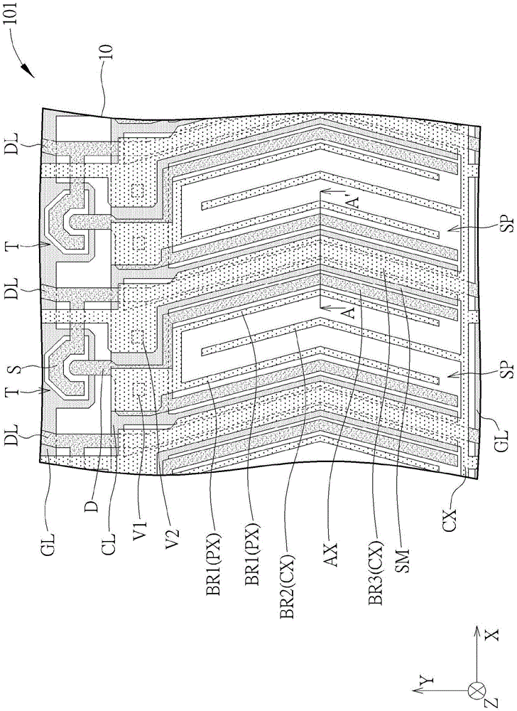
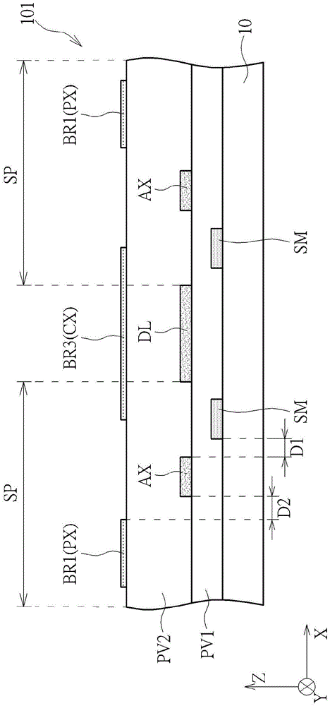
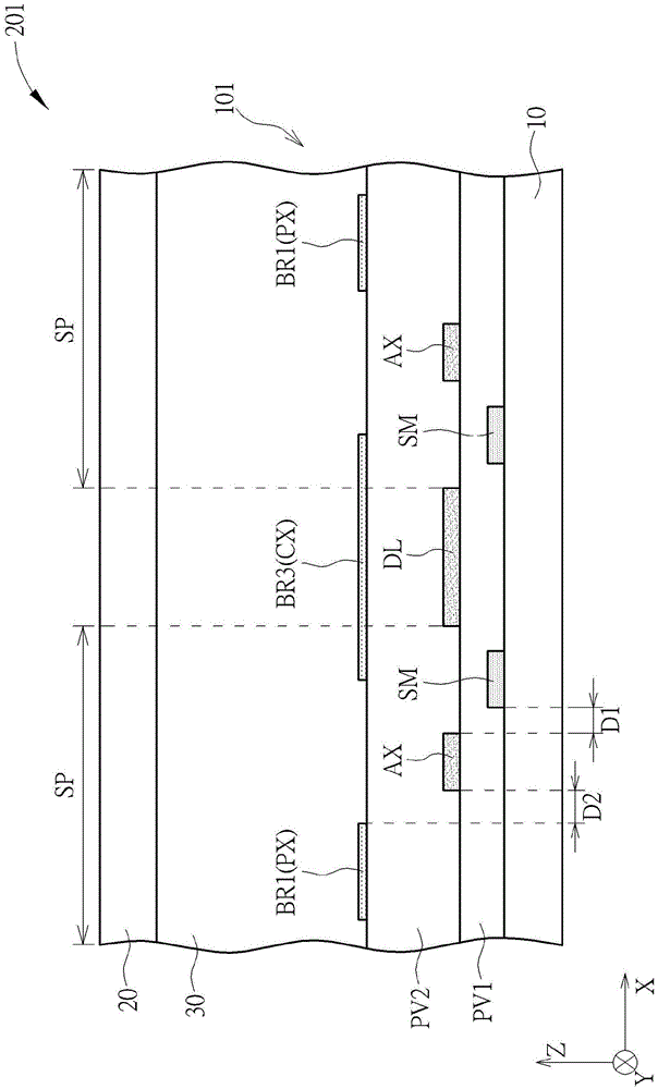
[0046] Please refer to figure 1 and figure 2 . figure 1 A schematic diagram of the array substrate according to the first embodiment of the present invention is shown. figure 2 for along figure 1 The cross-sectional schematic diagram drawn by the line A-A' in the middle. For the convenience of description, the drawings of the present invention are only schematic diagrams for easier understanding of the present invention, and the detailed proportions thereof can be adjusted according to design requirements. Such as figure 1 and figure 2 As shown, this embodiment provides an array substrate 101, including a substrate 10, a plurality o...


PUM


Abstract

The invention discloses an array substrate. The array substrate comprises a substrate, a data line, a grid electrode line, at least one pixel electrode, at least one common electrode, at least one shading pattern and at least one auxiliary electrode. The data line and the grid electrode line are arranged on the substrate and are staggered to define a pixel region. The pixel electrodes, the common electrodes, the shading patterns and the auxiliary electrodes are arranged on the substrate and are at least partially arranged in the pixel region. The pixel electrodes comprise at least one first branch electrode. The common electrodes comprise at least one second branch electrode. The first branch electrodes and the second branch electrodes are alternatively arranged in the first direction. The shading patterns are arranged between one data line adjacent to the pixel region and the first branch electrode in the first direction. The auxiliary electrodes are at least partially arranged between the first branch electrode and the shading patterns in the first direction, and the auxiliary electrodes and the pixel electrodes are electrically connected.

Description

technical field [0001] The present invention relates to an array substrate and a plane-switching liquid crystal display panel, especially to an array substrate and an array substrate that utilizes an auxiliary electrode having the same potential as the pixel electrode between a pixel electrode and a light-shielding pattern to improve crosstalk. In-plane switching LCD panel. Background technique [0002] With the continuous improvement of liquid crystal display technology, liquid crystal display panels have been widely used in flat-screen TVs, notebook computers, mobile phones and various types of consumer electronic products. In order to solve the shortcoming of the existing liquid crystal display with too small viewing angle, the industry has developed an in-plane switching (IPS) liquid crystal display whose main feature is that both the common electrode and the pixel electrode are arranged on the array substrate, and by The horizontal electric field generated by the commo...

Claims


Application Information

Patent Timeline
Patent Type & Authority Applications(China)
IPC IPC(8): G02F1/1343
CPCG02F1/134309G02F1/134363G02F1/134318G02F1/136218G02F1/13439G02F1/136209G02F1/136286G02F2201/121G02F2201/123
Inventor 叶于菱廖培钧黄俊儒
Owner AU OPTRONICS CORP
Learn More