Method and system for correcting signal missing in schematic diagram designing

An error correction system and schematic diagram technology, applied in the field of error correction, can solve the problems of forgetting to add page breaks, input errors and omissions of network labels, so as to solve the problem of missing signals and avoid the task of error checking.

Inactive Publication Date: 2016-06-22
PHICOMM (SHANGHAI) CO LTD
View PDF4 Cites 9 Cited by
  • Summary
  • Abstract
  • Description
  • Claims
  • Application Information

AI Technical Summary

Problems solved by technology

When the engineer is designing, due to the large system or many repeated revisions, the network label text may be entered incorrectly, missing or forgetting to add page breaks during multi-page design. In these cases, the netlist generated may be reflected in the PCB design. bring fatal error

Method used


Image

  • Method and system for correcting signal missing in schematic diagram designing
  • Method and system for correcting signal missing in schematic diagram designing
  • Method and system for correcting signal missing in schematic diagram designing

Examples


Embodiment Construction

[0037] The implementation of the present invention is described below through specific examples and in conjunction with the accompanying drawings, and those skilled in the art can easily understand other advantages and effects of the present invention from the content disclosed in this specification. The present invention can also be implemented or applied through other different specific examples, and various modifications and changes can be made to the details in this specification based on different viewpoints and applications without departing from the spirit of the present invention.

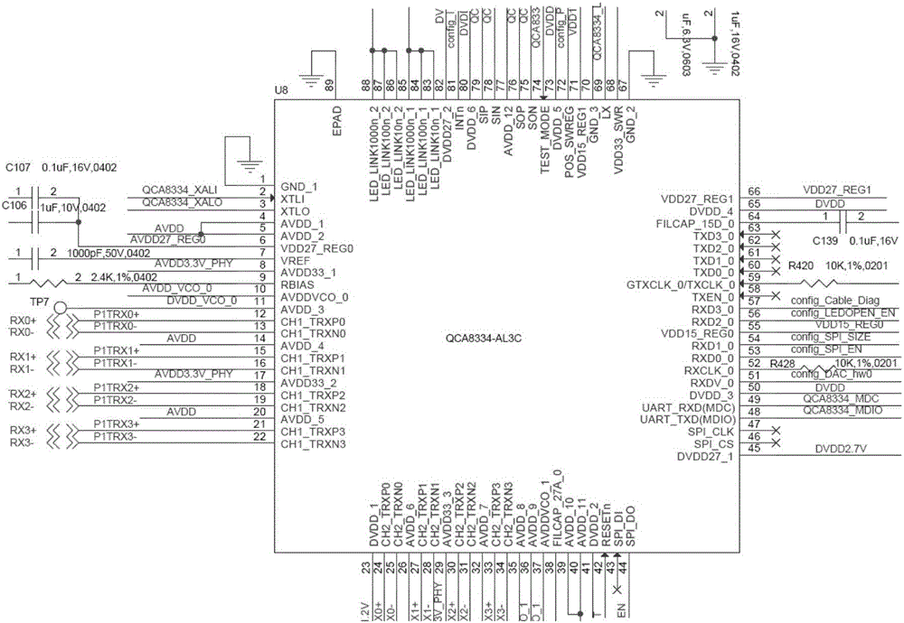
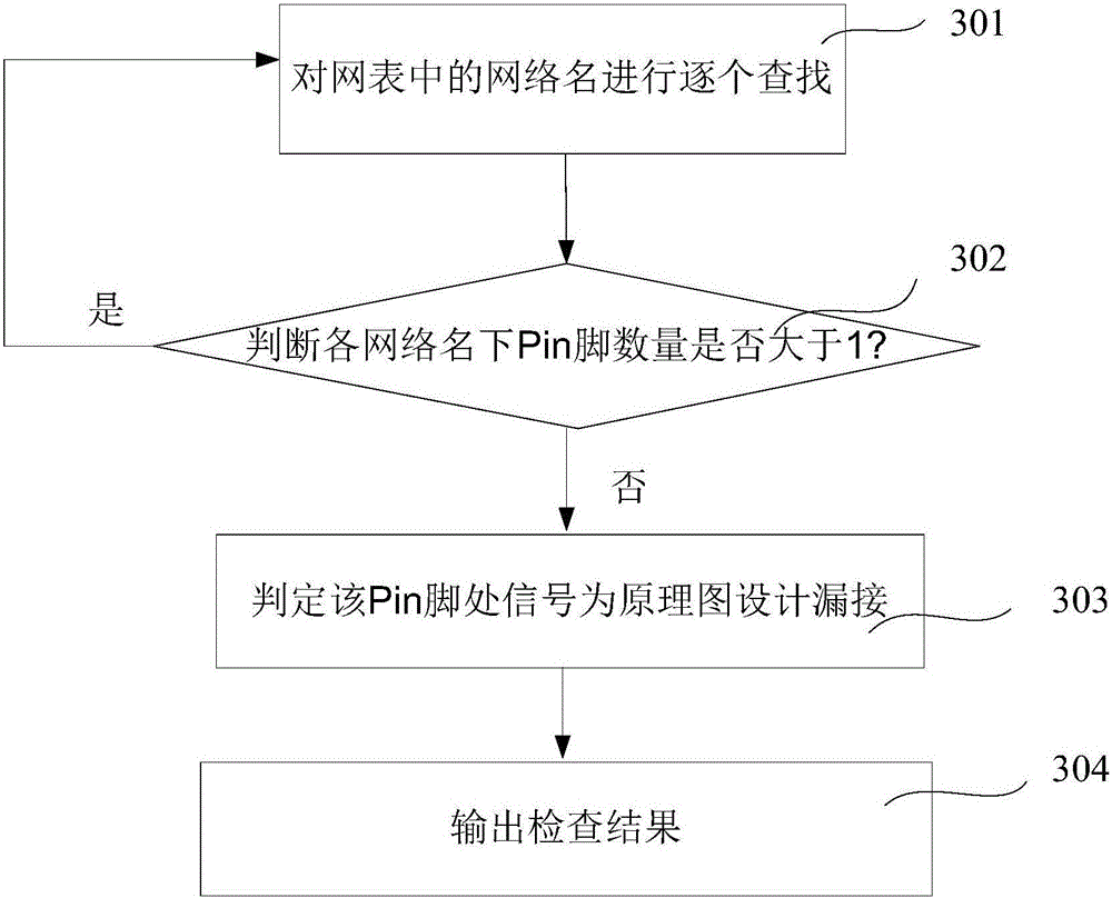
[0038] image 3 It is a flow chart of the steps of a method for correcting signal omissions in schematic diagram design in the present invention. Such as image 3 As shown, a method for error correction of signal omission in schematic diagram design of the present invention comprises the following steps:

[0039] In step 301, the net names in the net list are searched one by one.

[0040...


PUM


Abstract

The invention discloses a method and system for correcting signal missing in schematic diagram designing. The method includes the following steps that 1, network names in a net list are searched for one by one; 2, whether the number of Pins under each the network name is larger than one or not is judged; 3, if not, it is judged that the signal at the Pin position is missed in schematic diagram designing; 4, a check result is output. The situation of network name missing in a schematic diagram can be output directly, and missing connection, caused by carelessness or non-conforming software formats, of signal lines in schematic diagram designing of a hardware engineer is avoided.

Description

technical field [0001] The invention relates to an error correction method and system, in particular to a method and system for error correction of signal omissions in schematic diagram design. Background technique [0002] At present, there are a variety of schematic diagrams and PCB (Printed Circuit Board printed circuit board) design software in the electronics industry. Mature solution companies usually use Cadence's CarpturCIS to design schematic diagrams and Allegro software for PCB design operations. However, Cadence's CapturCIS does not have Check the functionality of a single point of connection. [0003] Now the common operation mode of design companies is that one person draws the schematic diagram and the other draws the PCB. A single person who draws a schematic diagram cannot check a single point of connection due to limited software capabilities. [0004] Such as figure 1 Shown is a schematic diagram of a common IC (Integrated Circuit, integrated circuit) c...

Claims


Application Information

Patent Timeline
Patent Type & Authority Applications(China)
IPC IPC(8): G06F17/50
CPCG06F30/392
Inventor 邓小斌
Owner PHICOMM (SHANGHAI) CO LTD
Why Eureka
Try Eureka