A method for manufacturing a deep-groove type super junction device

A manufacturing method and super junction technology, which can be used in semiconductor devices, electrical components, circuits, etc., can solve the problems of substrate doping and external expansion, and achieve the effect of improving reverse breakdown voltage.

Inactive Publication Date: 2016-06-22
SHANGHAI HUAHONG GRACE SEMICON MFG CORP
View PDF6 Cites 9 Cited by
  • Summary
  • Abstract
  • Description
  • Claims
  • Application Information

AI Technical Summary

Problems solved by technology

[0007] The technical problem to be solved in this application is to provide a method for manufacturing a deep trench type super junction device, which can solve the problem of dopant expansion in the substra

Method used


Image

  • A method for manufacturing a deep-groove type super junction device
  • A method for manufacturing a deep-groove type super junction device
  • A method for manufacturing a deep-groove type super junction device

Examples


Embodiment 1

[0048] A method for manufacturing a deep trench type super junction device, comprising the following steps:

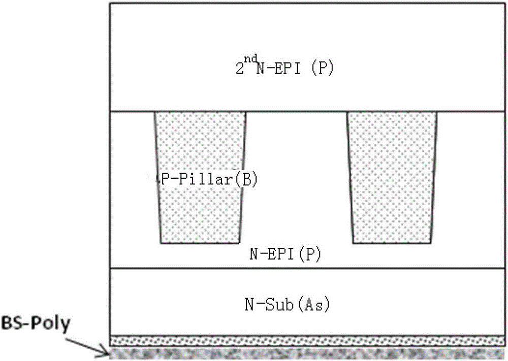
[0049]1. Form a first ONO (Oxide-Nitride-Oxide, oxide layer-nitride layer-oxide layer) dielectric layer 12 on the surface of the first N-type epitaxial layer (1stNEPI) 11 of the wafer (wafer), and the first ONO The dielectric layer 12 is respectively the third silicon oxide, the second silicon nitride, and the first silicon oxide from top to bottom, and the N-type heavily doped substrate (N-SUB) 10 under the first N-type epitaxial layer (NEPI) 11 , under the N-type heavily doped substrate 10 is a low temperature oxide (LTO) 13, under the low temperature oxide (LTO) 13 is a polysilicon layer (Poly) 14, and the low temperature oxide (LTO) 13 and the polysilicon layer (Poly) 14 are back seal, such as Figure 5 shown;

[0050] Two. Adopt the photolithography process to define the pattern of the first layer trench (Trench) on the first ONO dielectric layer 12 with photore...

Embodiment 2

[0062] Based on the manufacturing method of the deep trench super junction device in the first embodiment, the thickness of the low temperature oxide (LTO) in the back seal is about 1000 angstroms to 20000 angstroms, with a typical value of 5000 angstroms.

[0063] The thickness of the polysilicon layer (Poly) in the back seal is about 1000 angstroms to 20000 angstroms, with a typical value of 5000 angstroms.

Embodiment 3

[0065] Based on the manufacturing method of the deep trench type super junction device of the first embodiment, the typical ranges of the thicknesses of the first ONO dielectric layer and the second ONO dielectric layer: the thickness of the third silicon oxide is about 0.5-3um, and the thickness of the second nitride oxide is about 0.5-3um. The thickness of the silicon is about 100-1500 angstroms, and the thickness of the first silicon oxide is about 100-2000 angstroms, which can be increased or decreased according to actual needs.


PUM

PropertyMeasurementUnit
Thicknessaaaaaaaaaa
Thicknessaaaaaaaaaa
Thicknessaaaaaaaaaa

Abstract

The invention discloses a method for manufacturing a deep-groove type super junction device. A back-seal of a substrate is changed from the structure of Poly+LTO into LTO+Poly so as to prevent back-seal LTOs exposed outside from being removed by wet method technology. During growth of a second N-type epitaxial layer, the LTOs still exist owing to the protection by Poly. Elements heavily doped in the substrate will not spread and will not lead to abnormity of doping of the second N-type epitaxial layer. Under a condition that stress problems will not occur, problems of doping spreading in the substrate in a high-temperature growing process of the second N-type epitaxial layer can be solved, and electrical properties such as reverse breakdown voltages of the deep-groove type super junction device can be effectively improved.

Description

technical field [0001] The present application relates to semiconductor technology, in particular to a method for manufacturing a deep trench super junction device. Background technique [0002] The Chinese invention patent application with application publication number CN103035677A and application publication date of April 10, 2013 briefly introduces super junction MOSFET (metal-oxide field effect transistor) in the background technology part of its description. In addition to super junction MOSFETs, super junction devices also include super junction JFETs (junction field effect transistors), super junction Schottky diodes, super junction IGBTs (insulated gate bipolar transistors), etc. The common features of these super junction devices are Both have a superjunction structure. [0003] see figure 1 , which is a structural schematic diagram of an existing super-junction JFET, which has alternately arranged p-type pillars (pillars, also called vertical regions) and n-type...

Claims


Application Information

Patent Timeline
IPC IPC(8): H01L29/06
CPCH01L29/0607
Inventor 李昊
Owner SHANGHAI HUAHONG GRACE SEMICON MFG CORP
Why Eureka
Try Eureka