Structure of hybrid multi-core planar optical waveguide and coupling structure and coupling method thereof

A planar optical waveguide and coupling structure technology, applied in the field of optical waveguide coupling, can solve the problems of high packaging cost, difficulty in large-scale integration, complex process, etc., and achieve the effect of improving coupling efficiency and alignment tolerance

Active Publication Date: 2016-07-13
WUHAN TELECOMM DEVICES
View PDF3 Cites 9 Cited by
  • Summary
  • Abstract
  • Description
  • Claims
  • Application Information

AI Technical Summary

Problems solved by technology

[0002] The current mainstream 40G / 100G optical modules are basically based on free space coupling technology such as prisms, lenses, optical filters, etc., which are characterized by complex processes, active alignment with light, high packaging costs, and large-scale integration are very difficult

Method used


Image

  • Structure of hybrid multi-core planar optical waveguide and coupling structure and coupling method thereof
  • Structure of hybrid multi-core planar optical waveguide and coupling structure and coupling method thereof
  • Structure of hybrid multi-core planar optical waveguide and coupling structure and coupling method thereof

Examples


Embodiment 1

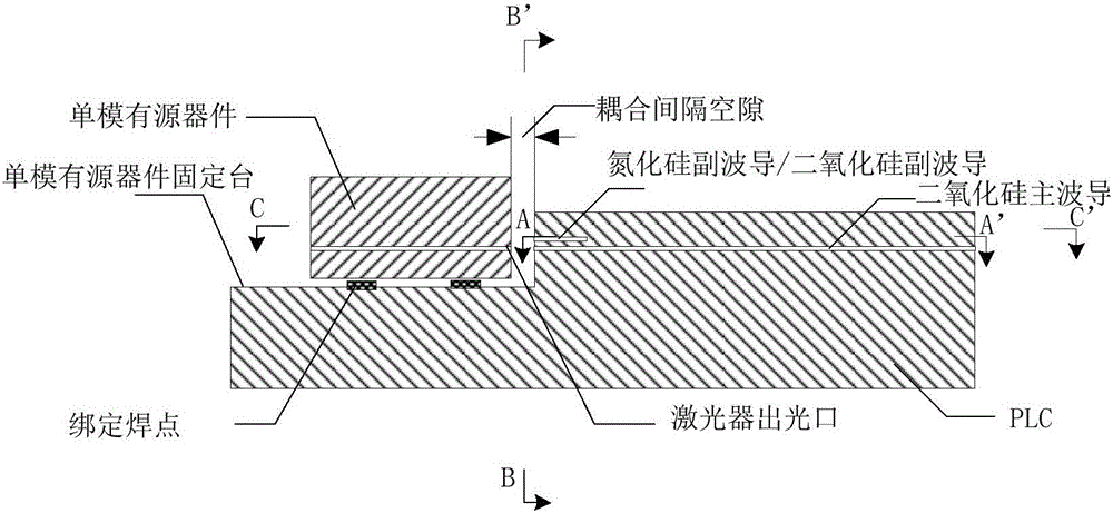
[0057] Embodiment 1 of the present invention provides a hybrid multi-core planar optical waveguide structure, such as Figure 1-4 The structure includes, specifically:

[0058] The planar optical waveguide includes a silicon dioxide main waveguide for transmitting optical signals, and a secondary waveguide for assisting light entering;

[0059] The secondary waveguide includes a silicon nitride secondary waveguide, and the silicon nitride secondary waveguide is in close contact with the silicon dioxide main waveguide.

[0060] Wherein, the silicon nitride secondary waveguide can be in various structural forms: for example, it is specifically a rectangular cubic structure, a positive ladder structure, an inverted ladder structure, and the like.

[0061] The hybrid multi-core waveguide proposed in this embodiment refers to adding a silicon nitride secondary waveguide other than the silicon dioxide main waveguide to the laser interface of the PLC to form a hybrid multi-core wave...

Embodiment 2

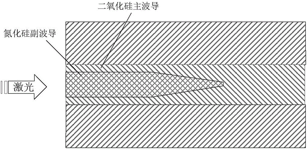
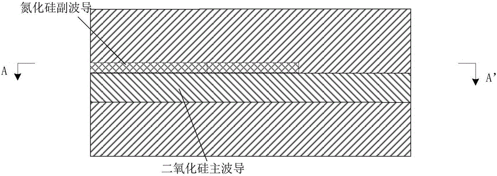
[0065] Based on the planar optical waveguide structure described in Embodiment 1, Embodiment 2 of the present invention specifically elaborates one of the optional sub-waveguide structures. Specifically, the sub-waveguide not only includes a silicon nitride sub-waveguide, but also includes Silica secondary waveguides, such as Figure 5 , Figure 6 , Figure 7 and Figure 8 As shown, the specific structure is described as follows:

[0066] The planar optical waveguide includes a silicon dioxide main waveguide for transmitting optical signals, and a secondary waveguide for assisting light entering;

[0067] Both the silicon nitride secondary waveguide and the silicon dioxide secondary waveguide are composed of a transition part and a cone part. The transition part is a rectangular cube extending toward the light transmission direction; A structure extending in the light transmission direction; wherein, the silicon nitride secondary waveguide is located on the upper surface o...

Embodiment 3

[0085] Based on the planar optical waveguide structure described in Embodiment 1, Embodiment 3 of the present invention specifically elaborates one of the optional secondary waveguide structures, such as Figure 10 , Figure 11 and Figure 12 As shown, specifically, the silicon nitride sub-waveguide is composed of two sub-sub-waveguides, wherein the first sub-sub-waveguide is located on the upper surface of the silicon dioxide main waveguide, and the second sub-sub-waveguide is located on the silicon dioxide The lower surface of the main waveguide.

[0086] In combination with the embodiment of the present invention, there is a preferred implementation solution, such as Figure 10 As shown, both the first sub-waveguide and the second sub-waveguide are composed of a transition part and a cone part, wherein the transition part is a rectangular cube extending toward the light transmission direction; wherein the cone part is the bottom surface and the transition part Convergenc...


PUM


Abstract

The invention relates to the technical field of optical waveguide coupling and provides a structure of a hybrid multi-core planar optical waveguide and a coupling structure and a coupling method thereof. The planar optical waveguide comprises a main silicon dioxide waveguide for transmitting optical signals and an auxiliary waveguide for assisting light incidence, wherein the auxiliary waveguide comprises an auxiliary silicon nitride waveguide body, and the auxiliary silicon nitride waveguide body tightly attaches to the main silicon dioxide waveguide. The hybrid multi-core planar optical waveguide is formed by adding the auxiliary silicon nitride/silicon dioxide waveguide body at the laser device interface end of a PLC besides the main silicon dioxide waveguide, and the coupling efficiency and alignment tolerance are improved. Due to the fact that the numerical aperture (NA) of the silicon nitride waveguide body is larger, the light-receiving capacity is better than that of the silicon dioxide waveguide. The effect of the hybrid multi-core waveguide is equivalent to the effect after a light inlet having stronger light receiving performance is added, all auxiliary waveguides disappear after a section of transition, accordingly light entering the added light inlet can be converged into the main waveguide in a waveguide parallel-coupling mode, and the purpose of improving the coupling efficiency and alignment tolerance is achieved.

Description

【Technical field】 [0001] The invention relates to the field of optical waveguide coupling technology, in particular to a hybrid multi-core planar optical waveguide structure and its coupling structure and coupling method. 【Background technique】 [0002] The current mainstream 40G / 100G optical modules are basically based on free space coupling technology such as prisms, lenses, optical filters, etc., which are characterized by complex processes, active alignment of light, high packaging costs, and large-scale integration are very difficult. [0003] On the other hand, photonic integration technology generally refers to active devices (lasers, detectors, optical amplifiers, optical modulators, etc.) ) integration to realize single-chip multi-functional optical device technology. Photonic integration technology is considered to be a powerful optical module technology in the near future and even in the future, especially in short-distance optical interconnection applications su...

Claims


Application Information

Patent Timeline
Patent Type & Authority Applications(China)
IPC IPC(8): G02B6/00G02B6/26
CPCG02B6/0028G02B6/26
Inventor 陈奔梁雪瑞朱虎胡百泉张玓刘成刚周日凯付永安孙莉萍马卫东余向红
Owner WUHAN TELECOMM DEVICES
Why Eureka
Try Eureka