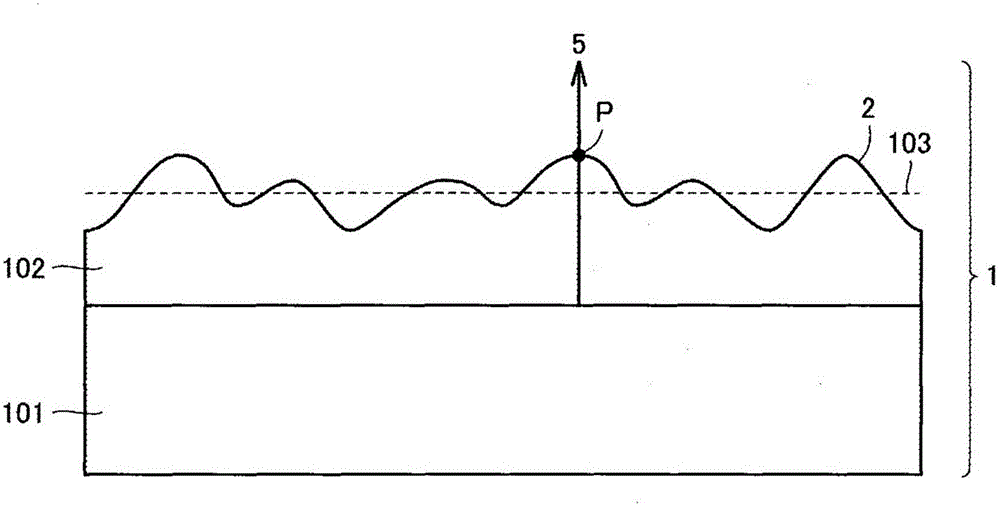
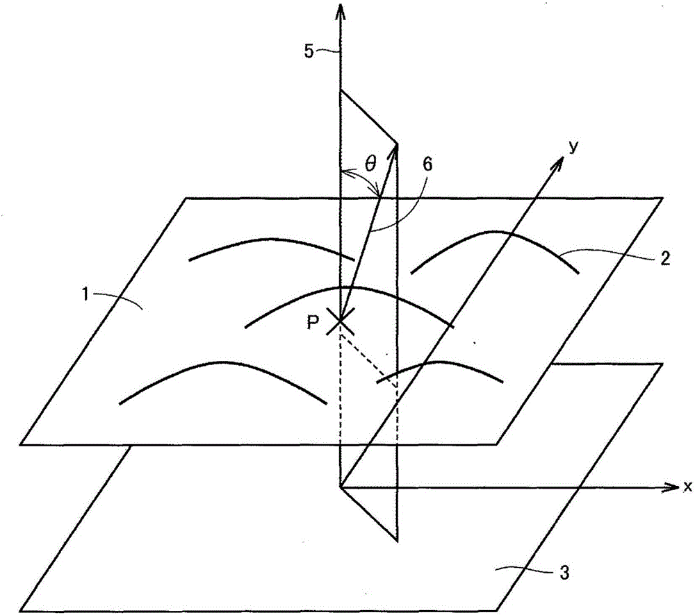
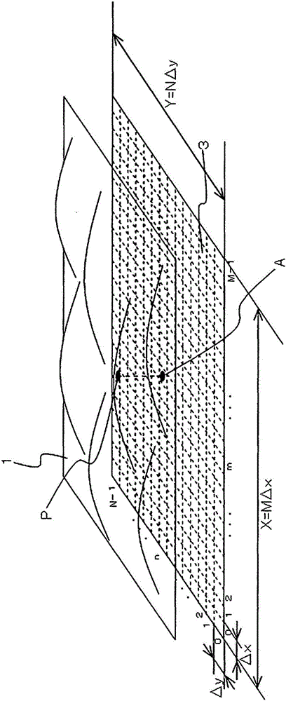
Antiglare film
An anti-glare film and transparent technology, applied in optics, instruments, nonlinear optics, etc., can solve the problem of reducing the anti-glare of the display surface, and achieve the effect of suppressing the occurrence of whitening and dazzling, and fully anti-glare.
- Summary
- Abstract
- Description
- Claims
- Application Information
AI Technical Summary
Problems solved by technology
Method used
Image

Examples
Embodiment 1
[0248] (Preparation of molds for anti-glare film production)
[0249] A material obtained by performing ballard copper plating on the surface of an aluminum roll (A6063 based on JIS) with a diameter of 300 mm was prepared. Ballard copper plating consists of copper plating / thin silver plating / surface copper plating, and the overall thickness of the plating is set to about 200 μm. The copper-plated surface was mirror-polished, and a photosensitive resin was applied and dried on the polished copper-plated surface to form a photosensitive resin film. Next, using the laser will be Figure 12 The pattern in which the pattern A shown above was repeatedly arranged was exposed on the photosensitive resin film, and it developed. Exposure and development were performed by laser using Laser Stream FX (manufactured by Think Laboratory). As the photosensitive resin film, a resin film containing a positive photosensitive resin was used. Here, pattern A is made by passing a pattern with r...
Embodiment 2
[0259] In addition to the use of lasers will be Figure 13 Mold B was produced in the same manner as in Example 1, except that the pattern in which the pattern B shown was repeatedly arranged was exposed on the photosensitive resin film, and the same as in Example 1 except that the mold A was replaced with the mold B. An anti-glare film was produced. This antiglare film was referred to as antiglare film B. Here, pattern B is made by passing a pattern with random luminance distribution through a plurality of Gaussian function type band-pass filters with an aperture ratio of 50%, and a one-dimensional power spectrum at a spatial frequency of 0.01 μm. -1 The intensity at Γ(0.01) is the same as that at the spatial frequency 0.02μm -1 The intensity Γ(0.02) at the ratio Γ(0.02) / Γ(0.01) is 0.12, at the spatial frequency 0.01μm -1 The intensity at Γ(0.01) is the same as that at the spatial frequency 0.1μm -1 The ratio of intensity Γ(0.1) at Γ(0.1) / Γ(0.01) is 11.85.
Embodiment 3
[0261] In addition to the use of lasers will be Figure 14 Except for exposing a pattern formed by repeating the pattern C shown on the photosensitive resin film, the mold C was produced in the same manner as the production of the mold A in Example 1, and the mold A was replaced with the mold C. An antiglare film was produced in the same manner as in Example 1. Let this antiglare film be antiglare film C. Here, pattern C is made by passing a pattern with random brightness distribution through a plurality of Gaussian function-type bandpass filters with an aperture ratio of 40%, and a one-dimensional power spectrum at a spatial frequency of 0.01 μm. -1The intensity at Γ(0.01) is the same as that at the spatial frequency 0.02μm -1 The intensity Γ(0.02) at the ratio Γ(0.02) / Γ(0.01) is 0.11, at the spatial frequency 0.01μm -1 The intensity at Γ(0.01) is the same as that at the spatial frequency 0.1μm -1 The ratio of intensity Γ(0.1) at Γ(0.1) / Γ(0.01) is 11.43.
PUM
| Property | Measurement | Unit |
|---|---|---|
| length | aaaaa | aaaaa |
| thickness | aaaaa | aaaaa |
| thickness | aaaaa | aaaaa |
Abstract
Description
Claims
Application Information
 - R&D
- Intellectual Property
- Life Sciences
- Materials
- Tech Scout
- Unparalleled Data Quality
- Higher Quality Content
- 60% Fewer Hallucinations
Browse by: Latest US Patents, China's latest patents, Technical Efficacy Thesaurus, Application Domain, Technology Topic, Popular Technical Reports.
© 2025 PatSnap. All rights reserved.Legal|Privacy policy|Modern Slavery Act Transparency Statement|Sitemap|About US| Contact US: help@patsnap.com