Wiring board with interposer and dual wiring structures integrated together and method of making the same

A wiring structure and circuit board technology, applied in multilayer circuit manufacturing, printed circuit manufacturing, circuit and other directions, can solve problems such as poor reliability of wafer-level connections, and achieve the goal of avoiding unconnected micro-blind holes and avoiding bending problems Effect

Inactive Publication Date: 2016-07-20
BRIDGE SEMICON
View PDF8 Cites 5 Cited by
  • Summary
  • Abstract
  • Description
  • Claims
  • Application Information

AI Technical Summary

Problems solved by technology

[0003] To make matters worse, since the coefficient of thermal expansion of semiconductor wafers (about 3 to 4 ppm for silicon) is lower than that of organic substrates (about 15 ppm for epoxy resin), it often causes interface stress due to mismatching coefficients of thermal expansion (CTE), making wafer-level connections (chip-level connection) poor reliability

Method used


Image

  • Wiring board with interposer and dual wiring structures integrated together and method of making the same
  • Wiring board with interposer and dual wiring structures integrated together and method of making the same
  • Wiring board with interposer and dual wiring structures integrated together and method of making the same

Examples


Embodiment 1

[0104] Figure 1-21 It is a diagram of a manufacturing method of a circuit board in an embodiment of the present invention, which includes an intermediate layer 15 , a first wiring structure 17 , a strengthening layer 20 and a second wiring structure 40 .

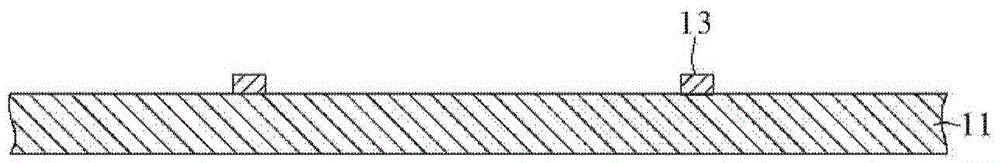
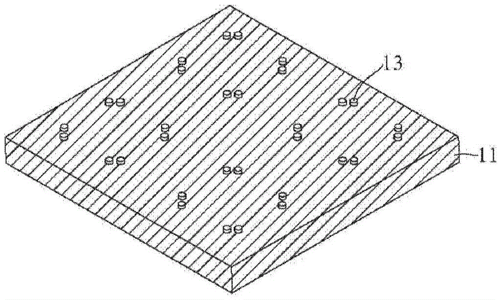
[0105] figure 1 and 2 They are respectively a cross-sectional view and a top perspective view of multiple sets of positioning elements 13 on the sacrificial carrier 11 . The sacrificial carrier 11 is typically made of copper, aluminum, iron, nickel, tin, stainless steel or other metals or alloys, but can also be made of any other conductive or non-conductive material. The thickness of the sacrificial carrier 11 is preferably 0.1 mm to 2.0 mm. The positioning member 13 protrudes from the top surface of the sacrificial carrier 11 and has a thickness of 5 to 200 microns. In this embodiment, the sacrificial carrier 11 has a thickness of 1.0 mm, and the positioning member 13 has a thickness of 50 microns. If a conductive sa...

Embodiment 2

[0131] Figure 23-51 It is a diagram of a circuit board manufacturing method according to another embodiment of the present invention, which includes the step of attaching the interposer semi-finished product to a sacrificial carrier.

[0132] For the purpose of brief description, any descriptions in the above-mentioned embodiment 1 that can be used for the same application are incorporated here, and it is not necessary to repeat the same descriptions.

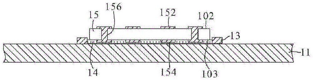
[0133] Figure 23 and 24 They are respectively a cross-sectional view and a bottom perspective view of the substrate 151 , which includes a first surface 101 , an opposite second surface 103 , and a blind hole 104 formed on the second surface 103 . The substrate 151 may be made of silicon, glass or ceramics, and has a thickness of 50 μm to 500 μm. The blind holes 104 have a depth of 25 microns to 250 microns. In this embodiment, the substrate 151 is a silicon wafer and has a thickness of 200 microns, and the blind hole 104...

Embodiment 3

[0159] Figures 52-56 It is a diagram of a circuit board manufacturing method according to another embodiment of the present invention, which does not use a carrier film, and the second wiring structure is further electrically coupled to the strengthening layer as a ground connection.


PUM


Abstract

A wiring board with integrated interposer and dual wiring structures is characterized in that an interposer and a first wiring structure are positioned within a through opening of a stiffener whereas a second wiring structure is disposed beyond the through opening of the stiffener. The mechanical robustness of the stiffener can prevent the wiring board from warping. The interposer provides primary fan-out routing for a semiconductor device to be assembled thereon. The first wiring structure can further enlarge the pad size and pitch of the interposer, whereas the second wiring structure not only provides further fan-out wiring structure, but also mechanically binds the first wiring structure with the stiffener.

Description

technical field [0001] The invention relates to a circuit board and a manufacturing method thereof, in particular to a circuit board in which an intermediary layer is interconnected to a double-wiring structure, and the integrated double-wiring structure is respectively located inside and outside the through-opening of the strengthening layer. Background technique [0002] For high-pin-count semiconductor chip packages and components, it is necessary to provide a high-density circuit board for the semiconductor chip to be placed on it, and then the chip I / O pads are routed to have a larger pad pitch to achieve a reliable board. Level assembly (board-level assembly). For example, various coreless substrates disclosed in US Pat. Nos. 9,060,455, 9,089,041, 8,859,912 and 8,797,757 are for fan-out routing of chips. Compared with the substrate with the core layer, the substrate without the core layer has the advantages of lower parasitic resistance, lower inductance and capacitan...

Claims


Application Information

Patent Timeline
Patent Type & Authority Applications(China)
IPC IPC(8): H01L23/498H01L21/48H05K3/46
CPCH01L21/4857H01L23/49805H01L23/49822H01L23/49894H05K3/4682H01L2224/16225H01L2224/32225H01L2224/73204H01L2924/0002H01L21/6836H01L2221/68345H01L21/486H01L23/5389H01L21/4853H01L21/6835H01L23/49827H01L23/49833H01L23/49838H01L2221/68381H01L2221/68309H01L2924/00H05K3/301H01L2221/68359
Inventor 林文强王家忠
Owner BRIDGE SEMICON
Why Eureka
Try Eureka