Circuit stacking structure

A stacking structure and circuit technology, applied to instruments, static indicators, etc., can solve the problems of wire layer 72 damage, increase manufacturing or maintenance costs, and inability to effectively protect wire layer 72 circuits, so as to avoid the increase of manufacturing or maintenance costs , Improve the pass rate and reduce the risk of damage

Active Publication Date: 2016-08-10
HANNSTAR DISPLAY NANJING +1
View PDF5 Cites 2 Cited by
  • Summary
  • Abstract
  • Description
  • Claims
  • Application Information

AI Technical Summary

Problems solved by technology

[0004] However, due to the differences in form between the raised portion 76 and the depressed portion 77 on the circuit stack structure 70 , such as differences in height or contact area, the protection layer 75 of the transition circuit region 60 is subjected to hard objects. When scratching, it is easy to cause the depression 77 to form a stress concentration point, or the bulge 76 bears excessive frictional force, so that the circuit of the wire layer 72 will not be effectively protected, and the risk of the wire layer 72 being damaged will be increased, thereby increasing the manufacturing process. or repair costs

Method used


Image

  • Circuit stacking structure
  • Circuit stacking structure
  • Circuit stacking structure

Examples


Embodiment Construction

[0020] The following will clearly illustrate the spirit of the present invention with the accompanying drawings and detailed descriptions. After those skilled in the art understand the embodiments of the present invention, they can be changed and modified by the techniques taught in the present invention without departing from the present invention. spirit and scope.

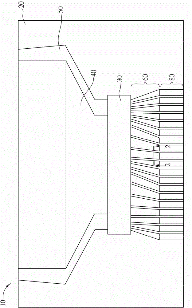
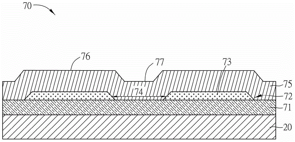
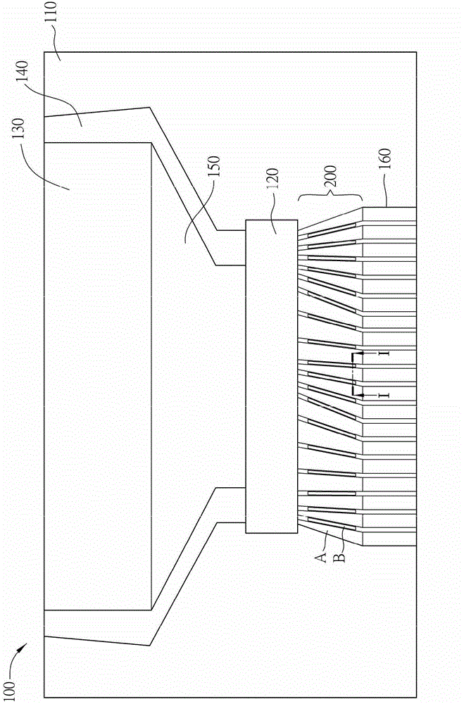
[0021] The present invention provides an active element array substrate and its circuit stacking structure, which are used to shorten the difference between the raised part and the depressed part in the known structure, such as the difference in height difference, friction degree or contact area, so as to reduce the difference. The transition line area is subject to the destructive force generated by the passing of hard objects, reducing the risk of damage to the lines within it.

[0022] In the following, several embodiments will be disclosed based on the above description to further clarify the spirit of the p...


PUM


Abstract

The invention discloses a circuit stacking structure, wherein the circuit stacking structure includes a wire layer, a supporting part and a protection layer. The wiring layer includes a plurality of metal wires arranged separately, and the supporting parts are respectively located in the gaps between any two adjacent metal wires, and are electrically insulated from the metal wires. The protection layer covers the wire layer and the supporting part, and through the support of the supporting part, the area corresponding to the supporting part on the top surface of the protective layer is flush with the area corresponding to each metal line.

Description

technical field [0001] The present invention relates to a circuit stacking structure, and in particular to a circuit stacking structure of an active element array substrate. Background technique [0002] figure 1 It is a partial top view of a known active device array substrate 10 . Such as figure 1 As shown, the active device array substrate 10 includes a glass substrate 20 , a driving chip 30 , a plurality of data lines 40 and a plurality of scan lines 50 . The data lines 40 , the scan lines 50 and the driving chip 30 are all disposed on the glass substrate 20 . The driver chip 30 is coupled to the data line 40 and the scan line 50 on the one hand, and connected to a flexible circuit board pad area 80 through a transition line area 60 on the glass substrate 20 on the other hand. The transition line area 60 is located between the driver chip 30 and the pad area 80 of the flexible circuit board, and the wiring in it continues from the pad area 80 of the flexible circuit ...

Claims


Application Information

Patent Timeline
Patent Type & Authority Applications(China)
IPC IPC(8): G09G3/20
Inventor 吴健豪李懿庭
Owner HANNSTAR DISPLAY NANJING
Why Eureka
Try Eureka