Display panel and manufacture method thereof

A technology for display panels and display substrates, which is applied in the manufacturing of semiconductor/solid-state devices, semiconductor devices, electrical components, etc., can solve the problems of affecting the display effect, complicated manufacturing process, and increased cathode voltage drop, and achieves the convenience of narrow frame design, Simple craftsmanship

Active Publication Date: 2016-08-10
WUHAN TIANMA MICRO ELECTRONICS CO LTD +1
View PDF7 Cites 33 Cited by
  • Summary
  • Abstract
  • Description
  • Claims
  • Application Information

AI Technical Summary

Problems solved by technology

[0004] Depend on figure 1 It can be seen that in the existing OELD display panel, the second via hole Via2 needs to be provided on the pixel definition layer 116 in the frame area B, so as to connect the cathode 114 to the wiring 115, the manufacturing process is complicated, and the setting of the second via hole Via2 It is not convenient for the design of narrow frame of OLED d

Method used


Image

  • Display panel and manufacture method thereof
  • Display panel and manufacture method thereof
  • Display panel and manufacture method thereof

Examples


Embodiment Construction

[0028] The technical solutions in the embodiments of the present invention will be clearly and completely described below with reference to the accompanying drawings in the embodiments of the present invention. Obviously, the described embodiments are only a part of the embodiments of the present invention, but not all of the embodiments. Based on the embodiments of the present invention, all other embodiments obtained by those of ordinary skill in the art without creative efforts shall fall within the protection scope of the present invention.

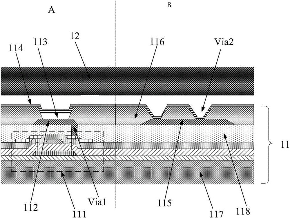
[0029] As described in the background art, in the prior art, in order to electrically connect the cathode 114 of the OLED display panel with the trace 115 for supplying the cathode voltage, it is necessary to punch holes to form the second through hole Via2, which is complicated in manufacturing process and high in manufacturing cost. And when the second through hole Via2 is arranged in the frame area B, in order to reduce the contact ...


PUM


Abstract

The invention discloses a display panel and a manufacture method thereof. The display panel comprises a display area and a border area. The display panel comprises a cover plate and a display substrate, wherein the cover plate and the display substrate are oppositely arranged. The cover plate comprises a first conductive layer. The display substrate comprises a TFT substrate and a pixel definition layer which is arranged on one side, which faces the cover plate, of the TFT substrate. The pixel definition layer comprises an opening area and an opening-free area. The opening area is provided with a light-emitting function layer. A first electrode is arranged between the light-emitting function layer and the TFT substrate. The opening-free area is provided with a raised structure facing the cover plate. A second electrode layer is arranged on the light-emitting function layer and the surface of the raised structure. The second electrode layer is electrically connected with the first conductive layer at a position corresponding to the raised structure. Wiring is arranged in a preset area, which is corresponding to the border area, of the display substrate. The wiring is used for providing the work voltage of the second electrode layer. The first conductive layer is electrically connected with the wiring. According to the display panel, the width of the border area is reduced, and the problem of voltage drop of the second electrode layer is avoided.

Description

technical field [0001] The present invention relates to the technical field of display devices, and more particularly, to a display panel and a manufacturing method thereof. Background technique [0002] With the continuous development of science and technology, more and more electronic devices with display function are widely used in people's daily life and work, which brings great convenience to people's daily life and work, and has become an indispensable part of the current people. important tool that is missing. The main component of the electronic device to realize the display function is the display panel, and the OLED display panel is one of the current mainstream display panels. [0003] refer to figure 1 , figure 1 It is a schematic structural diagram of a common OLED panel in the prior art. The OLED display panel includes: a cover plate 12 and an array substrate 11 which are arranged oppositely. The OLED display panel has a display area A and a frame area B. ...

Claims


Application Information

Patent Timeline
IPC IPC(8): H01L27/32H01L51/56
CPCH10K59/88H10K71/00
Inventor 马志丽钱栋
Owner WUHAN TIANMA MICRO ELECTRONICS CO LTD
Why Eureka
Try Eureka