Routing structure of liquid crystal display panel and manufacture method of routing structure

A technology of a liquid crystal display panel and a manufacturing method, which are applied in nonlinear optics, instruments, optics, etc., can solve the problems of affecting the display effect, poor alignment effect, inability to input different common voltages to the liquid crystal display panel, etc., so as to improve the display effect. Effect

Inactive Publication Date: 2016-08-24
TCL CHINA STAR OPTOELECTRONICS TECH CO LTD
View PDF6 Cites 16 Cited by
  • Summary
  • Abstract
  • Description
  • Claims
  • Application Information

AI Technical Summary

Problems solved by technology

[0005] The object of the present invention is to provide a wiring structure of a liquid crystal display panel and a manufacturing method thereof, so as to solve the wiring structure of the prior art, which cannot input different common voltages to each liquid crystal display panel, resulting in poor alignment effect and affecting display Technical issues with effects

Method used


Image

  • Routing structure of liquid crystal display panel and manufacture method of routing structure
  • Routing structure of liquid crystal display panel and manufacture method of routing structure
  • Routing structure of liquid crystal display panel and manufacture method of routing structure

Examples


Embodiment Construction

[0021] The following descriptions of the various embodiments refer to the accompanying drawings to illustrate specific embodiments in which the present invention can be practiced. The directional terms mentioned in the present invention, such as "up", "down", "front", "back", "left", "right", "inside", "outside", "side", etc., are for reference only The orientation of the attached schema. Therefore, the directional terms used are used to illustrate and understand the present invention, but not to limit the present invention. In the figures, structurally similar units are denoted by the same reference numerals.

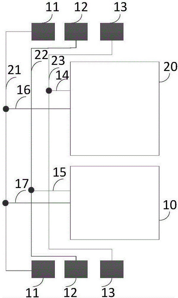
[0022] Please refer to figure 1 , figure 1 It is a schematic diagram of a wiring structure of an existing liquid crystal display panel.

[0023] Such as figure 1 As shown, the existing liquid crystal display panel wiring structure, the first liquid crystal display panel 10 and the second liquid crystal display panel 20, and the common curing pad 11, the spare curi...


PUM


Abstract

The invention provides a routing structure of a liquid crystal display panel and a manufacture method of the routing structure. The routing structure comprises a public curing cushion, a curing bus, at least one auxiliary curing cushion, and at least one curing auxiliary line, wherein the public curing cushion is used for receiving total public voltage; the curing bus is used for transmitting the total public voltage to one liquid crystal display panel; each auxiliary curing cushion is used for receiving sub public voltage; each liquid crystal display panel in the rest liquid crystal display panels corresponds to an auxiliary curing cushion; each curing auxiliary cushion corresponds to a curing auxiliary line; the curing auxiliary line is connected with a curing bus, and is used for transmitting sub public voltage to each liquid crystal display panel in the rest liquid crystal display panels, so as to input different public voltage to each liquid crystal display panel. The routing structure of the liquid crystal display panel and the manufacture method of the routing structure can ensure that the alignment effect of each display panel is optimal.

Description

【Technical field】 [0001] The invention relates to the technical field of displays, in particular to a wiring structure of a liquid crystal display panel and a manufacturing method thereof. 【Background technique】 [0002] For small and medium-sized liquid crystal displays, two or more liquid crystal display panels are generally placed on the same mask (Mask) during curing. Since alignment needs to be performed before curing, it will be pre-set around the panels. There is a wiring structure. [0003] In the existing wiring structure, only one common curing pad is reserved, that is, all panels share a common curing pad, and the common curing pad is used to receive a common voltage. When panels of different sizes are placed on the same photomask, different common voltages are required when the panels of different sizes are aligned. However, since the existing panels are connected to the same common curing pad, different voltages cannot be input to the panels. After the mask i...

Claims


Application Information

Patent Timeline
Patent Type & Authority Applications(China)
IPC IPC(8): G02F1/1345G02F1/1333
CPCG02F1/1333G02F1/1345
Inventor 冯托
Owner TCL CHINA STAR OPTOELECTRONICS TECH CO LTD
Why Eureka
Try Eureka