Embedded touch array substrate, driving method thereof, and display device

A technology of an array substrate and a driving method, which is applied in the directions of instruments, calculations, and electrical digital data processing, etc., can solve problems such as voltage jumps and lower image quality of liquid crystal display panels, and achieve the goal of avoiding voltage jumps and improving display quality Effect

Active Publication Date: 2019-02-26
BOE TECH GRP CO LTD
View PDF4 Cites 0 Cited by
  • Summary
  • Abstract
  • Description
  • Claims
  • Application Information

AI Technical Summary

Problems solved by technology

With this simple VCOM division method, when the display stage and the touch stage are switched to each other, VCOM will inevitably produce a voltage jump, thereby reducing the display quality of the LCD panel.

Method used


Image

  • Embedded touch array substrate, driving method thereof, and display device
  • Embedded touch array substrate, driving method thereof, and display device
  • Embedded touch array substrate, driving method thereof, and display device

Examples


Embodiment Construction

[0031] The following will clearly and completely describe the technical solutions in the embodiments of the present invention with reference to the accompanying drawings in the embodiments of the present invention. Obviously, the described embodiments are only part of the embodiments of the present invention, not all of them. Based on the embodiments of the present invention, all other embodiments obtained by persons of ordinary skill in the art without making creative efforts belong to the protection scope of the present invention.

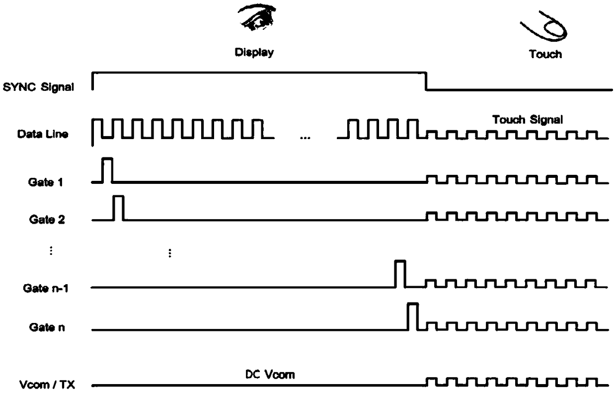
[0032] In order to solve the problem that the VCOM voltage jump phenomenon affects the display quality of the liquid crystal display panel, in the prior art, the data (Data) signal input to the display IC is first processed and then input to the liquid crystal display panel for use, but This method cannot fundamentally solve the problem of VCOM voltage jump, and the effect of improving the display quality is still very limited.

[0033] Based on ...


PUM


Abstract

The invention discloses an embedded touch array substrate, a driving method thereof, and a display device. Wherein, the in-cell touch array substrate includes a common electrode layer, and the common electrode layer includes: a common electrode of the pixel part, corresponding to all pixel areas of the in-cell touch array substrate, and in the touch stage, the pixel part The common electrodes receive common electrode signals; the peripheral part of the common electrodes corresponds to at least part of the non-pixel regions except all pixel regions, and in the touch stage, the peripheral part of the common electrodes receives touch sensing signals. Through the present invention, the effect of improving the display quality of the liquid crystal display panel is achieved.

Description

technical field [0001] The present invention relates to the field of display technology, in particular to an in-cell touch array substrate, a driving method thereof, and a display device. Background technique [0002] At present, the touch panel and the liquid crystal display panel of most touch devices are set independently, the touch panel is set on the liquid crystal display panel, and there is a physical space between the liquid crystal display panel and the touch panel, therefore, in the liquid crystal display External light is reflected on the upper surface of the panel and the lower surface of the touch panel, which reduces the visibility of the LCD panel in brightly lit environments such as outdoors. If the visibility of the touch panel can be realized, the integration of the two can also realize the thinning and lightening of the entire display panel. [0003] Under the requirement of this technical development, the In Cell touch technology emerges and develops rap...

Claims


Application Information

Patent Timeline
Patent Type & Authority Patents(China)
IPC IPC(8): G06F3/041G06F3/044G02F1/1333G02F1/1343G02F1/1362
CPCG02F1/13338G02F1/134309G02F1/136286G06F3/0412G06F3/044G06F2203/04111G06F3/04184G06F3/0443G02F1/1333G02F1/1343G02F1/1362G06F3/0416
Inventor 彭敏王泓荆耀秋
Owner BOE TECH GRP CO LTD
Why Eureka
Try Eureka