Supercharge Your Innovation With Domain-Expert AI Agents!

PCB (Printed Circuit Board) and mobile terminal provided with same

A PCB board and hole section technology, applied in the field of mobile terminals, can solve problems such as connection failure, high cost of via holes, voids, etc., and achieve the effects of improving overall quality, saving copper materials, and improving production efficiency

Inactive Publication Date: 2016-09-07
GUANGDONG OPPO MOBILE TELECOMM CORP LTD
View PDF10 Cites 0 Cited by
  • Summary
  • Abstract
  • Description
  • Claims
  • Application Information

AI Technical Summary

Problems solved by technology

In the related art, in order to realize the electrical connection between the conductive layers in the multi-layer PCB board, it is usually necessary to make stacked holes between multiple conductive layers, and to make stacked holes between multiple conductive layers requires electroplating and filling of the via holes , so that not only the cost of the via hole is high, but also the electroplating filling process cannot achieve a completely flat copper surface, and there will be a certain depression above the via hole, which is prone to problems such as connection failure or voids.

Method used


Image

  • PCB (Printed Circuit Board) and mobile terminal provided with same
  • PCB (Printed Circuit Board) and mobile terminal provided with same

Examples


Embodiment Construction

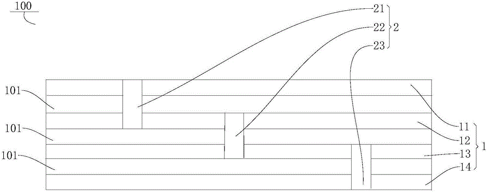
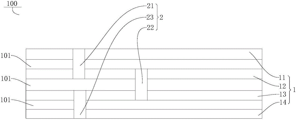
[0024] Embodiments of the present invention are described in detail below, examples of which are shown in the drawings, wherein the same or similar reference numerals designate the same or similar elements or elements having the same or similar functions throughout. The embodiments described below by referring to the figures are exemplary only for explaining the present invention and should not be construed as limiting the present invention.

[0025] In describing the present invention, it is to be understood that the terms "upper", "lower", "front", "rear", "left", "right", "vertical", "horizontal" etc. indicate an orientation or The positional relationship is based on the orientation or positional relationship shown in the drawings, which is only for the convenience of describing the present invention and simplifying the description, rather than indicating or implying that the referred device or element must have a specific orientation, be constructed and operated in a specif...


PUM


Abstract

The invention discloses a PCB (Printed Circuit Board) and a mobile terminal provided with same. The PCB comprises multiple layers of conducting layers which are mutually stacked and a conductive through hole used for connecting two conducting layers which are far away from each other, wherein the conductive through hole comprises a plurality of sub-hole sections which are connected along a vertical direction in sequence; two adjacent sub-hole sections are connected through one conducting layer, and two adjacent sub-hole sections are staggered with each other. According to the PCB of the invention, through separate setting of the sub-hole sections of the conductive through hole, routing on each conducting layer can be flexibly avoided during drilling, and an electroplating filling process can be omitted during production of the PCB, so that the copper material is saved and the production efficiency is improved.

Description

technical field [0001] The invention relates to the technical field of mobile terminals, in particular to a PCB board and a mobile terminal with the PCB board. Background technique [0002] Vias are an important part of the PCB board, some of which are used to complete the connection of the signal lines of each layer, some are used to connect the power layer, some are used to connect the ground wire, and some are used for heat dissipation. In the related art, in order to realize the electrical connection between the conductive layers in the multi-layer PCB board, it is usually necessary to make stacked holes between multiple conductive layers, and to make stacked holes between multiple conductive layers requires electroplating and filling of the via holes , so that not only the cost of the via hole is high, but also the electroplating filling process cannot achieve a completely flat copper surface, and there will be a certain depression above the via hole, which is prone to ...

Claims


Application Information

Patent Timeline
IPC IPC(8): H05K1/11
CPCH05K1/115H05K2201/09563H05K2201/096
Inventor 范艳辉
Owner GUANGDONG OPPO MOBILE TELECOMM CORP LTD
Features
  • R&D
  • Intellectual Property
  • Life Sciences
  • Materials
  • Tech Scout
  • Unparalleled Data Quality
  • Higher Quality Content
  • 60% Fewer Hallucinations
Learn More