Wafer bonding method
A wafer bonding and wafer technology, which is applied in the manufacture of electrical components, electrical solid devices, semiconductor/solid devices, etc., can solve the problems of poor uniformity of bonded wafers, improve performance, improve uniformity, and optimize bonds. combined twist effect
- Summary
- Abstract
- Description
- Claims
- Application Information
AI Technical Summary
Problems solved by technology
Method used
Image

Examples
Embodiment Construction
[0025] The wafer bonding method proposed by the present invention will be further described in detail below with reference to the accompanying drawings and specific embodiments. According to the following description and claims, the advantages and features of the present invention will be clearer. It should be noted that the drawings are in a very simplified form and all use imprecise proportions, which are only used to conveniently and clearly assist in explaining the purpose of the embodiments of the present invention.
[0026] Such as figure 1 As shown, the present invention discloses a wafer bonding method, including:
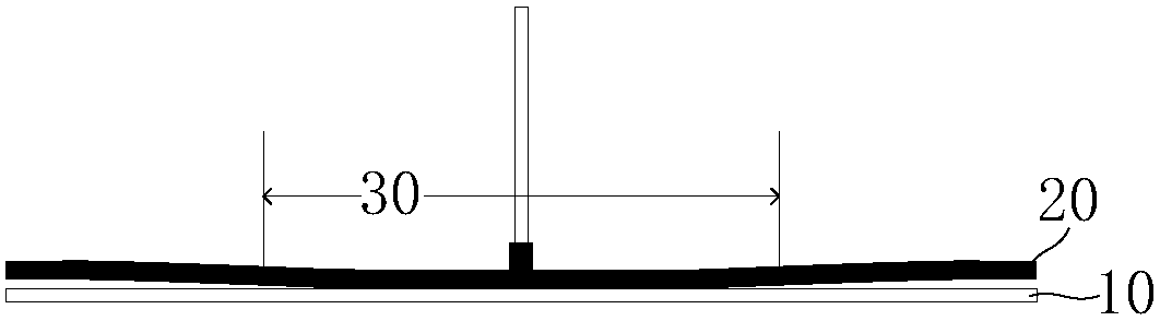
[0027] Step S10: Provide a first wafer 10 and a second wafer 20;
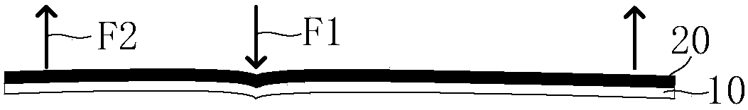
[0028] Step S20: Provide a negative pressure environment, stack the first wafer 10 and the second wafer 20, and apply at least one pressure to the center of the first wafer 10 and the second wafer 20 On area 30.
[0029] Press below figure 1 The shown process is combined with the schematic diagram...
PUM
 Abstract
Description
Claims
Application Information
 - R&D
- Intellectual Property
- Life Sciences
- Materials
- Tech Scout
- Unparalleled Data Quality
- Higher Quality Content
- 60% Fewer Hallucinations
Browse by: Latest US Patents, China's latest patents, Technical Efficacy Thesaurus, Application Domain, Technology Topic, Popular Technical Reports.
© 2025 PatSnap. All rights reserved.Legal|Privacy policy|Modern Slavery Act Transparency Statement|Sitemap|About US| Contact US: help@patsnap.com