Planarization method

A planarization method and chemical mechanical technology, applied in the field of planarization, can solve the problems of increasing process cost, etc., and achieve the effect of reducing process cost and avoiding load effect

Active Publication Date: 2016-10-05
SEMICON MFG INT (SHANGHAI) CORP
View PDF5 Cites 1 Cited by
  • Summary
  • Abstract
  • Description
  • Claims
  • Application Information

AI Technical Summary

Problems solved by technology

[0005] However, the reverse process using the existing photoresist will undoubtedly increase the process cost due to the need to form a photoresist layer and separately make a photomask suitable for the reverse process

Method used


Image

  • Planarization method
  • Planarization method
  • Planarization method

Examples


Embodiment Construction

[0025] In order to make the purpose, technical solution and advantages of the present invention more clear, the present invention will be further described in detail below with reference to the accompanying drawings and examples.

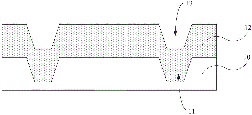
[0026] The invention provides a method for manufacturing a semiconductor device, such as figure 2 shown, including:

[0027] providing a semiconductor substrate to be polished, the semiconductor substrate is formed with a first recess;

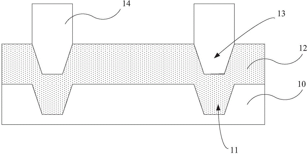
[0028] Covering and forming a first filling layer on the semiconductor substrate, the first filling layer completely fills the first depression, and the first filling layer is formed with a second depression corresponding to the position of the first depression;

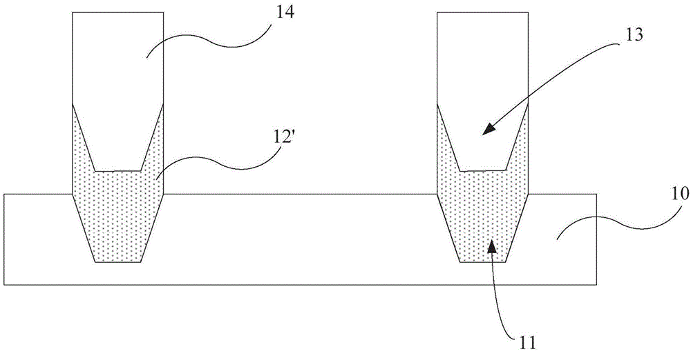
[0029] Depositing a second filling layer on the surface of the first filling layer, the second filling layer completely fills the second depression and covers the surface of the first filling layer;

[0030] performing a first chemical mechanical polish...


PUM


Abstract

The present invention provides a planarization method. The photoresist in the traditional reverse process is replaced by the second filling layer to cover the surface of the first filling layer, and the second depression in the first filling layer is removed by the first chemical mechanical polishing. and using the second filling layer in the second recess as a mask, use the first etching to remove most of the first filling layer, after removing the second filling layer in the second recess, The remaining first filling layer is removed by the second chemical mechanical polishing, thereby reducing the process cost while avoiding the severe loading effect produced by the chemical mechanical polishing process.

Description

technical field [0001] The invention relates to the technical field of semiconductors, in particular to a planarization method. Background technique [0002] In the manufacture of existing semiconductor devices, in order to obtain a planarized surface, a chemical mechanical polishing process is often used. The chemical mechanical polishing process mainly uses the chemical action of the polishing liquid and the physical action of the rotation of the grinding head to make the object to be polished comprehensively planarized. [0003] In practical applications, chemical mechanical polishing is susceptible to load effects due to the impact of the grinding object. Specifically, for a wafer with depressions formed on the surface, since the density of depressions formed on the surface of the wafer and the opening area of ​​the depressions are not the same, the polishing rates of different regions of the wafer surface during chemical mechanical polishing are different. Generally s...

Claims


Application Information

Patent Timeline
Patent Type & Authority Applications(China)
IPC IPC(8): H01L21/3105H01L21/321
Inventor 姜海涛
Owner SEMICON MFG INT (SHANGHAI) CORP
Why Eureka
Try Eureka