A metal groove etching method

A metal trench, metal technology, applied in the manufacturing of electrical components, circuits, semiconductor/solid-state devices, etc., can solve the problem that the load effect is difficult to meet the process requirements, and achieve the effect of good contact, reduced load effect, and avoidance of load effect.

Active Publication Date: 2018-10-16
SHANGHAI HUALI MICROELECTRONICS CORP
View PDF4 Cites 0 Cited by
  • Summary
  • Abstract
  • Description
  • Claims
  • Application Information

AI Technical Summary

Problems solved by technology

[0016] In actual operation, the groove shape is relatively easy to meet the process requirements, but without affecting the groove shape, due to the different characteristics and settings of the machine, the load effect is often difficult to meet the process requirements

Method used


Image

  • A metal groove etching method
  • A metal groove etching method
  • A metal groove etching method

Examples


Embodiment Construction

[0050] In order to make the content of the present invention clearer and easier to understand, the content of the present invention will be further described below in conjunction with the accompanying drawings. Of course, the present invention is not limited to this specific embodiment, and general replacements known to those skilled in the art are also covered within the protection scope of the present invention.

[0051] Secondly, the present invention is described in detail by means of schematic diagrams. When describing the examples of the present invention in detail, for the convenience of explanation, the schematic diagrams are not partially enlarged according to the general scale, which should not be used as a limitation of the present invention.

[0052] Embodiments of the present invention will be further described below in conjunction with the accompanying drawings.

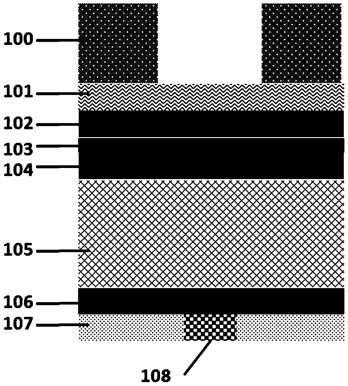
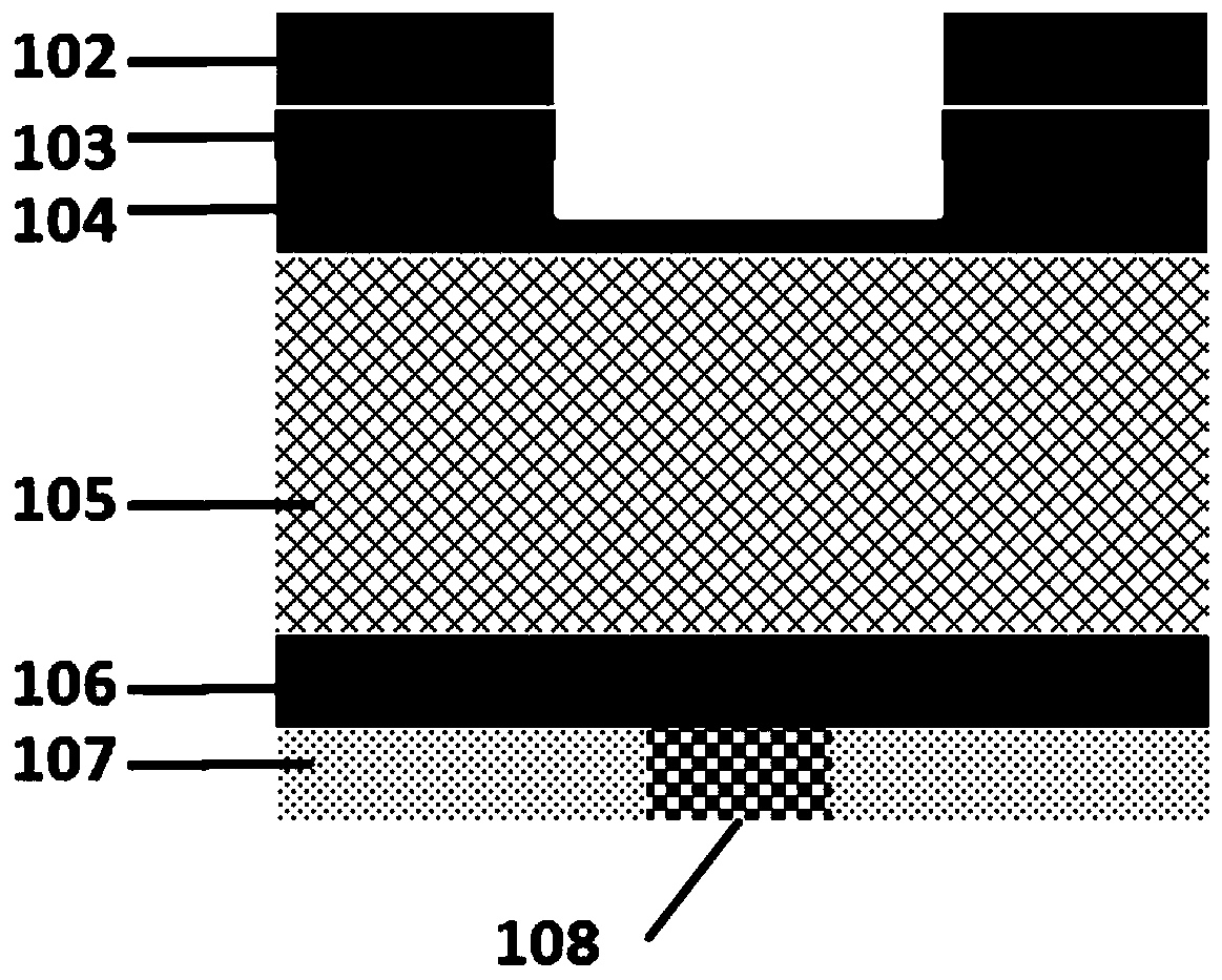
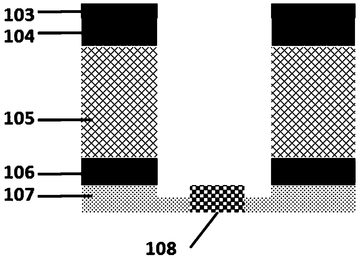
[0053] The front-end process of this embodiment adopts the standard 40 / 45nm and 28 / 32nm technology n...


PUM


Abstract

The invention provides a first layer metal trench etching method. The ILD dielectric of a contact hole layer in a wafer front-layer process is SiO2, and contact hole WCMP is completed. The method comprises the steps that etching stop layers are deposited; a Low-k dielectric layer is deposited; by introducing the mask plate and the shrinkage plate of a first layer metal trench, metal hard mask etching and Low-k dielectric layer etching are separated; by using the difference between etching selection ratio of different materials, two times of etching stop at the etching stop layers which are respectively located at the top and the bottom of the Low-k dielectric layer; and great uniformity of wet etching is used to reduce an etching loading effect. Compared with a first layer metal trench dry etching method in the prior art, the method provided by the invention has the advantages that a better optimization loading effect is realized without affecting the morphology of the first layer metal trench; the consistency of process parameters of first layer metal is ensured; and the uniformity of process parameters of the whole device is optimized.

Description

technical field [0001] The invention relates to the technical field of integrated circuit manufacturing, in particular to a metal trench etching method. Background technique [0002] The integrated circuit manufacturing process is constantly developing, the feature size of the device is also decreasing, and the nanoscale and sub-nanoscale technology nodes are becoming more and more mature. Starting from the 45 / 40nm technology node, the dielectric material ILD in the back-end process basically uses a low-k (Low-k) dielectric film with a large porosity, and its mechanical properties are correspondingly greatly weakened as the porosity increases. Studies have proved that the mechanical properties of dielectric materials play an important role in the process of defect generation after CMP. Specifically, it means that improving the mechanical properties of the dielectric material surface can significantly reduce the mechanical damage caused by CMP. Therefore, the industry introd...

Claims


Application Information

Patent Timeline
Patent Type & Authority Patents(China)
IPC IPC(8): H01L21/768H01L21/311
CPCH01L21/31144H01L21/76802
Inventor 任洪瑞盖晨光黄君张里艳
Owner SHANGHAI HUALI MICROELECTRONICS CORP
Why Eureka
Try Eureka