Integrated method of raise source leakage structure complementary metal-oxide-semiconductor transistor (CMOS) and Bipolar device

A technology that improves source and drain and integrates methods. It is applied in the direction of semiconductor devices, semiconductor/solid-state device manufacturing, and electrical components. It can solve problems such as shallowing, epitaxial single crystal height restrictions, and slow impurity diffusion. It can expand the process window, Improve the effect of short channel effect and relax the design size

Active Publication Date: 2015-04-08
SHANGHAI HUAHONG GRACE SEMICON MFG CORP
View PDF4 Cites 0 Cited by
  • Summary
  • Abstract
  • Description
  • Claims
  • Application Information

AI Technical Summary

Problems solved by technology

The raised source and drain are generally grown by selective epitaxial silicon single crystal, and then the source and drain junctions are formed by ion implantation. The depth of the source and drain junctions formed in this way will also be correspondingly shallower, thereby improving the short channel effect. This structure Because high-dose implantation is generally relatively shallow, and the diffusion of impurities in silicon single crystals is slow, the height of epitaxial single crystals is limited

Method used


Image

  • Integrated method of raise source leakage structure complementary metal-oxide-semiconductor transistor (CMOS) and Bipolar device
  • Integrated method of raise source leakage structure complementary metal-oxide-semiconductor transistor (CMOS) and Bipolar device
  • Integrated method of raise source leakage structure complementary metal-oxide-semiconductor transistor (CMOS) and Bipolar device

Examples


specific Embodiment

[0047] The inventive method specifically comprises the steps:

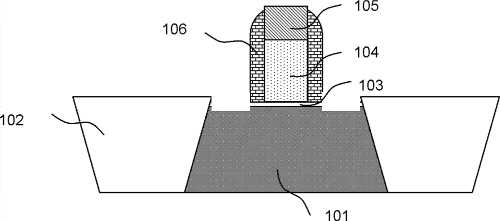
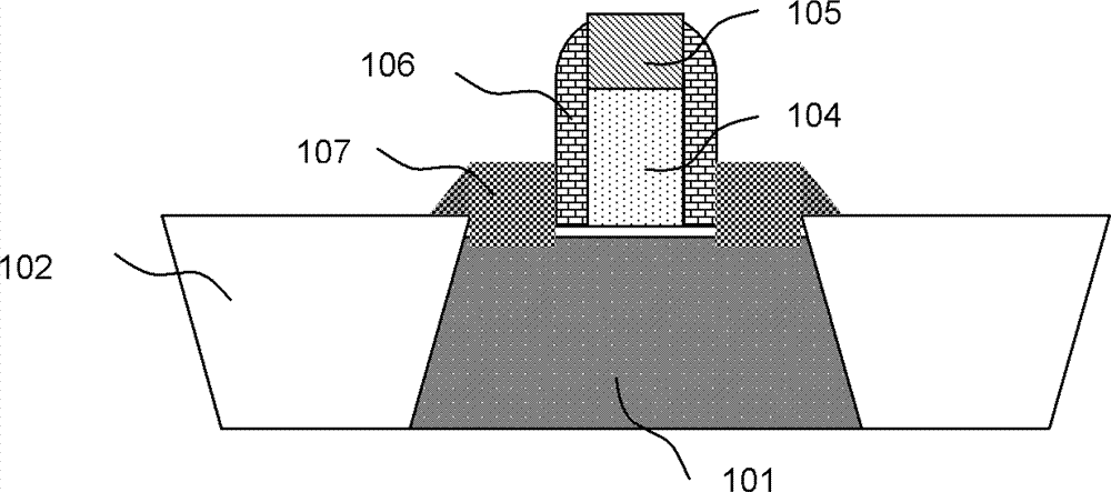
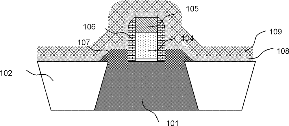
[0048] 1. If figure 1 As shown, the definition of the CMOS gate pattern and the formation of sidewalls are completed according to the traditional process flow. The CMOS regional structure includes an active region 101, a shallow trench isolation region 102, and a gate structure, wherein the gate structure is 20 from bottom to top. A gate oxide layer 103 of -70 angstroms, a gate polysilicon 104 of about 2000 angstroms, a top dielectric film 105 of about 1000 angstroms, and a gate spacer 106. On the basis of the traditional shallow trench isolation (STI) structure, a traditional gate structure is formed. After the LDD is implanted, the gate spacer 106 is formed. When the gate spacer 106 is formed, anisotropic etching is used to make silicon The active area 101 of the substrate has a loss of about 20-100 Angstroms. Because the silicon substrate is damaged during the etching process, polysilicon will grow in the so...


PUM


Abstract

The invention discloses an integrated method of a raise source leakage structure complementary metal-oxide-semiconductor transistor (CMOS) and a Bipolar device. The integrated method of the raise source leakage structure CMOS and the Bipolar device comprises forming a grid structure on a traditional shallow groove isolation structure, wherein a certain etch quantity of a silicon substrate is caused by side wall etch, using selective epitaxy to develop polycrystalline silicon in a source leakage area so as to form a raise source leakage area, depositing dielectric film again to protect a CMOS area; forming a polycrystalline silicon side wall after base polycrystalline silicon etch is carried out, removing dielectric film of the CMOS area, and keeping dielectric film under the polycrystalline silicon side wall; using emitting electrode polycrystalline silicon as expansion of the raise source leakage area to a shallow trench isolation (STI) area and a connecting line of a CMOS local area, coating a layer of filling materials after imaging is carried out, carrying out backward etch on the filling materials and the emitting electrode polycrystalline silicon above the source leakage area, and stopping etch on the dielectric film; at last, removing the filling materials and an etch stopping layer, and finishing source leakage injection, follow-up contact holes and a metal connecting line technology. The integrated method of the raise source leakage structure CMOS and the Bipolar device has the advantages of being capable of effectively reducing the size from an active area to a grid, increasing amount of transistors in unit area, enlarging a technology window, reducing source leakage parasitic capacitance, and improving a short-channel effect.

Description

technical field [0001] The invention belongs to the field of semiconductor integrated circuit manufacturing, and in particular relates to an integration method of CMOS (complementary metal oxide semiconductor field effect transistor) and Bipolar (bipolar transistor) devices with raised source-drain structure. Background technique [0002] Reducing the design size of the active area (AA) and the gate (gate) can effectively reduce the parasitic capacitance of the source and drain, increase the speed of the device, and at the same time reduce the area of ​​the device, so that there are more devices per unit area. However, this design size is limited by the design size of the contact hole and the process capability of the contact hole registration, and the process window and the device size become two factors that restrict each other. [0003] Another problem is that as the device size continues to shrink, the effective channel length decreases, which is known to cause the short...

Claims


Application Information

Patent Timeline
Patent Type & Authority Patents(China)
IPC IPC(8): H01L21/70H01L21/336H01L21/28H01L21/265
Inventor 刘鹏
Owner SHANGHAI HUAHONG GRACE SEMICON MFG CORP
Why Eureka
Try Eureka