Preparation method for resistive random access memory

A resistive memory, plasma technology, applied in electrical components and other directions, can solve the problems of large erasing voltage, large resistance change range in high resistance state, and poor resistance stability, so as to reduce the erasing voltage and improve stability. , the effect of high reactivity

Active Publication Date: 2013-12-11
ZHEJIANG UNIV
View PDF3 Cites 17 Cited by
  • Summary
  • Abstract
  • Description
  • Claims
  • Application Information

AI Technical Summary

Problems solved by technology

[0006] The atomic layer deposition technology for the preparation of resistive variable memory in the existing research is mainly thermal atomic layer deposition technology and plasma enhanced atomic layer deposition (PEALD) technology. The preparation process of the two technologies is based on the periodic cycle deposition of ALD: thermal Atomic layer deposition technology uses water vapor as the second precursor to react with the first precursor, for example, J. Zhang et al. (Structural, optical, electrical and resistive switching properties of ZnO thin films deposited by thermal and plasma- enhanced atomic layer deposition, Appl.Surf.Sci.282,395 (2013)) uses thermal atomic layer deposition technology to prepare zinc oxide thin film, which shows good electrical conductivity, and the resistivity can reach 10 -3 Ω.cm order, but the ZnO thin film prepared by this method does not have resistance switching characteristics; the plasma-enhanced atomic layer deposition technology uses plasma as the second precursor to react with the first precursor, for example, J. Zhang et al. (Bipolar resistive switching characteristics of low temperature grown ZnO thin films by plasma-enhanced atomic layer deposition, Appl. Phys. Lett, 102, 012113 (2013)) used plasma-enhanced atomic layer deposition technology to prepare zinc oxide thin films to The Al / PEALD-ZnO / Pt resistive variable memory prepared by the thin film has a resistance ratio between a high resistance state and a low resistance state greater than 10 3 , but there are also problems of poor stability of resistance switching and large range of resistance changes in high resistance state
[0007] Other thin films prepared by ALD technology (such as aluminum oxide, titanium oxide, etc.) also have problems such as poor stability of resistive switching, large erase and write voltage, and large range of resistance changes in high-resistance states, which limit the application of ALD technology in resistive switching. Wide range of applications in the field of memory

Method used


Image

  • Preparation method for resistive random access memory
  • Preparation method for resistive random access memory
  • Preparation method for resistive random access memory

Examples


Embodiment 1

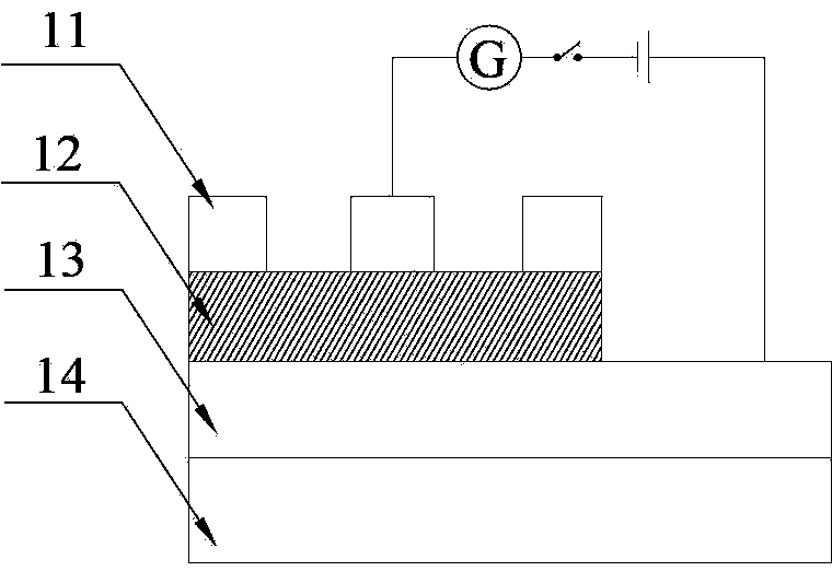
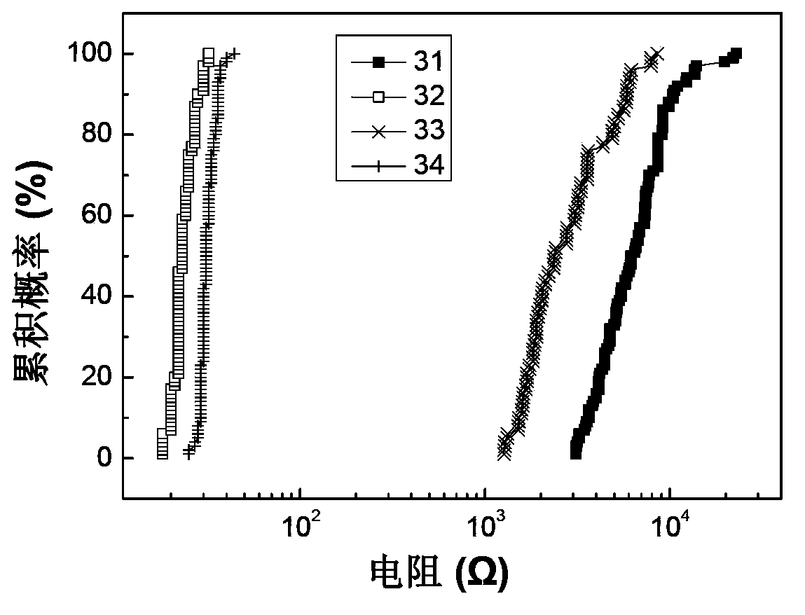
[0064] 1) Using magnetron sputtering method on SiO 2 (300nm) / Si(100) substrate surface prepared inert metal Pt bottom electrode, the thickness of the obtained bottom electrode was 150nm, the preparation temperature was 150°C, the main deposition gas was argon, the pressure was 0.5Pa, and the sputtering power was 300W.

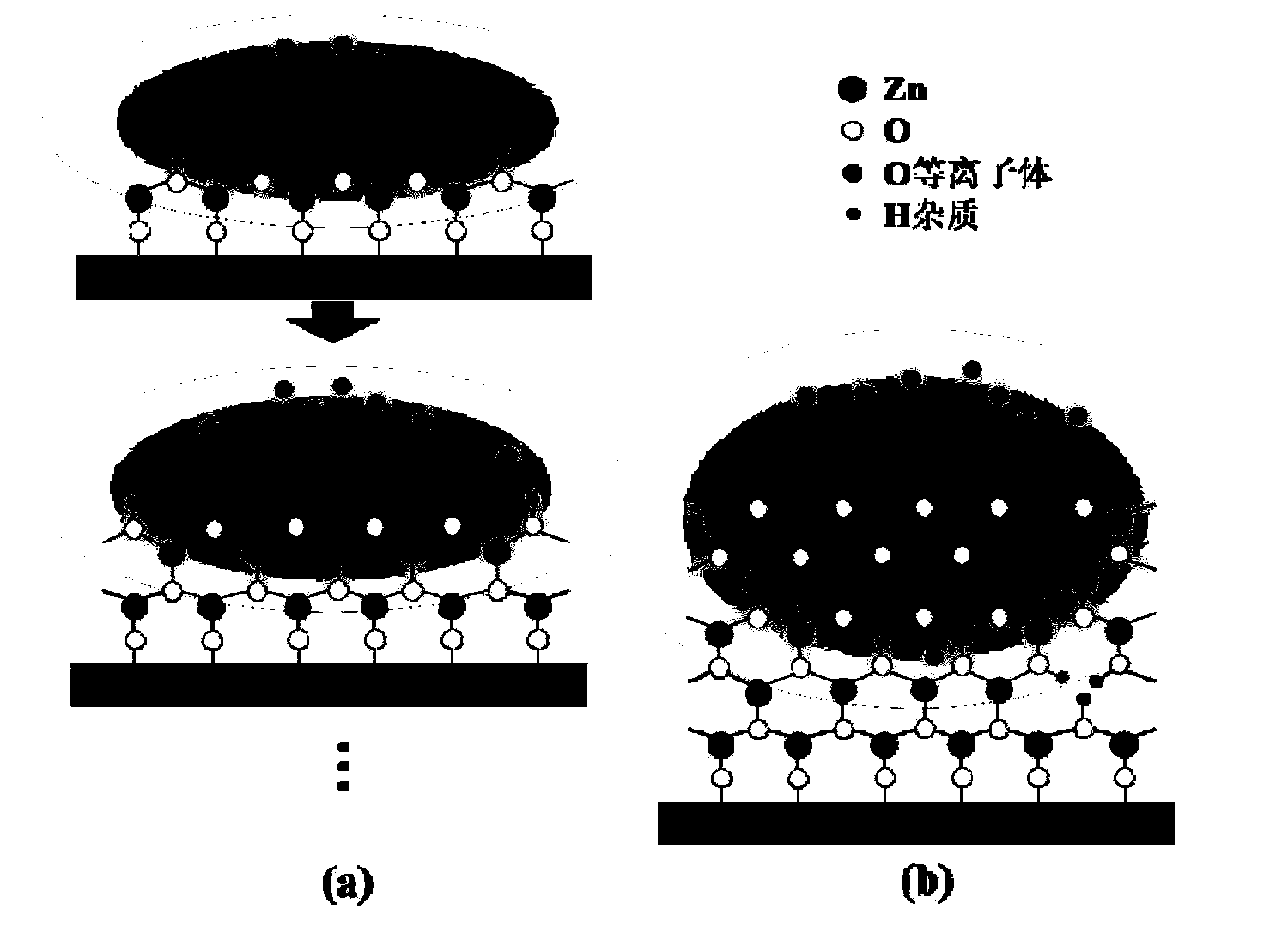
[0065] 2) Using the in-situ plasma enhanced thermal atomic layer deposition method, diethyl zinc was used as the first precursor, water vapor was used as the second precursor, and argon was used as the cleaning gas. After thermal atomic layer deposition, the Pt bottom electrode was first A single-layer zinc oxide film was formed on the film, and then the film was subjected to in-situ plasma treatment with oxygen plasma, and repeated 250 cycles to finally obtain a zinc oxide film with a thickness of about 42nm. The temperature of the Pt bottom electrode was 150°C; the flow rate of argon carrier gas was 20 sccm; the deposition and processing pressure was 1 Torr; ...

Embodiment 2

[0074] 1) Using magnetron sputtering method on SiO 2 (300nm) / Si(100) substrate surface prepared inert metal Pt bottom electrode, the thickness of the obtained bottom electrode was 150nm, the preparation temperature was 150°C, the main deposition gas was argon, the pressure was 0.5Pa, and the sputtering power was 300W.

[0075] 2) Using the in-situ plasma enhanced thermal atomic layer deposition method, diethyl zinc was used as the first precursor, water vapor was used as the second precursor, and argon was used as the cleaning gas. After thermal atomic layer deposition, the Pt bottom electrode was first A single-layer zinc oxide film was formed on the film, and then the film was subjected to in-situ plasma treatment with oxygen plasma, and repeated 250 cycles to finally obtain a zinc oxide film with a thickness of about 42nm. The temperature of the Pt bottom electrode is 150° C.; the flow rate of argon carrier gas is 20 sccm, the deposition and processing pressure of the react...

Embodiment 3

[0081] The aluminum oxide thin film resistive memory is prepared by thermal atomic layer deposition technology, and hydrogen plasma is used for in-situ treatment, including the following steps:

[0082] 1) Using magnetron sputtering method on SiO 2 (300nm) / Si(100) substrate surface prepared inert metal bottom electrode Pt, the thickness of the obtained bottom electrode was 150nm, the preparation temperature was 150°C, the main deposition gas was argon, the pressure was 0.5Pa, and the sputtering power was 300W.

[0083] 2) Using atomic layer deposition technology, using trimethylaluminum as the first precursor, water vapor as the second precursor, and argon as the cleaning gas, a single layer is first formed on the Pt bottom electrode after thermal atomic layer deposition Aluminum oxide thin film, and then use hydrogen plasma to process in-situ plasma on the thin film, repeat 200 cycles, finally obtain aluminum oxide thin film, the thickness of the thin film is about 20nm. The...


PUM

PropertyMeasurementUnit
thicknessaaaaaaaaaa
electrical resistivityaaaaaaaaaa
thicknessaaaaaaaaaa

Abstract

The invention discloses a preparation method for a resistive random access memory. The resistive random access memory comprises a bottom electrode, a resistance change dielectric layer material and a top electrode which are assembled in sequence. Preparation of the resistance change dielectric layer material includes the following steps that firstly, a first precursor, first inert gas, a second precursor and second inert gas are fed into a reactor in order, and a monolayer metallic oxide film is deposited on the bottom electrode through a cycle of hot atomic layer deposition; secondly, a plasma enhancement process is carried out on the film; finally, the steps are carried out circularly and alternately. In the preparation process of a resistance change dielectric layer, a brand new in-situ plasma enhancement hot atomic layer deposition technology is brought in, so the surface appearance and defects of the metallic oxide film can be adjusted on a large scale; the resistive random access memory obtained through the preparation method can achieve precision control over device resistance switching characteristics to enable the device switch ratio and erase/write voltage to be adjusted, and has excellent resistance change stability.

Description

technical field [0001] The invention relates to the field of semiconductors, in particular to a preparation method of a resistive variable memory. Background technique [0002] With the advent of the 32nm technology node of the integrated circuit process, the traditional Flash memory has encountered a series of problems. Among them, the most important problem is that as the thickness of the tunnel oxide layer becomes smaller and smaller, the leakage of charges becomes more and more serious. The more serious it is, it will directly affect the data retention performance of the Flash memory. In recent years, various new non-volatile memories have been developed rapidly, such as ferroelectric memory, magnetic memory, phase change memory and resistive change memory (RRAM). Realize the advantages of high-density storage and become the most competitive "universal" non-volatile memory of the next generation. [0003] RRAM uses the resistive layer material to have the resistance sw...

Claims


Application Information

Patent Timeline
Patent Type & Authority Applications(China)
IPC IPC(8): H01L45/00
Inventor 张启龙张剑杨辉
Owner ZHEJIANG UNIV
Why Eureka
Try Eureka