Method for detecting bottom outline of contact plug

A detection method and technology for contact plugs, which are used in semiconductor/solid-state device testing/measurement, electrical components, semiconductor/solid-state device manufacturing, etc., can solve problems such as inability to obtain photos and inability to obtain contact plug bottom contour detection results, etc. Achieve the effect of reducing charge trapping effect, good test environment and reducing error

Active Publication Date: 2011-11-23
WUHAN XINXIN SEMICON MFG CO LTD +1
View PDF3 Cites 17 Cited by
  • Summary
  • Abstract
  • Description
  • Claims
  • Application Information

AI Technical Summary

Problems solved by technology

The detection process of using SEM to measure the wafer including the doped region 18 is as follows: firstly, the first dielectric layer 13 and the second dielectric layer 15 are removed by using an acid solution, and the metal layer 16 and the contact plug 14 are also removed thereupon, Since the contact plug 14 is partly locate

Method used


Image

  • Method for detecting bottom outline of contact plug
  • Method for detecting bottom outline of contact plug
  • Method for detecting bottom outline of contact plug

Examples


no. 1 example

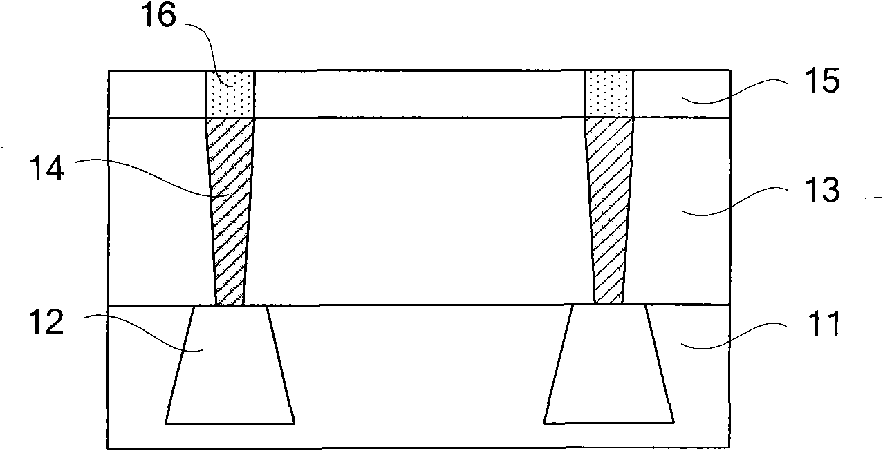
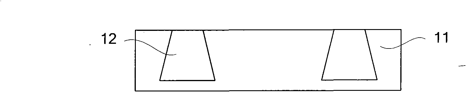
[0042] reference Figure 5A , First provide a wafer; the wafer includes: a semiconductor substrate 21 formed with an active region 22; a first dielectric layer 23 on the semiconductor substrate 21; penetrating through the first dielectric layer 23 and with the The contact plug 24 electrically connected to the source region 22; the second dielectric layer 25 formed on the first dielectric layer 23 and the contact plug 24; and the second dielectric layer 25 penetrates the second dielectric layer 25 and is in contact with the The metal layer 26 to which the plug 24 is electrically connected.

[0043] Wherein, the material of the first dielectric layer 23 and the second dielectric layer 25 is one or a combination of silicon oxide or silicon nitride, and the material of the contact plug 24 is tungsten, copper, or aluminum. The contact plug 24 may be a trapezoidal plug.

[0044] reference Figure 5B , The metal layer 26 and the second dielectric layer 25 are removed by chemical mechanic...

no. 2 example

[0054] reference Figure 6A , First provide a wafer; the wafer includes: a semiconductor substrate 31 formed with an active region 32; a first dielectric layer 33 on the semiconductor substrate 31; penetrating the first dielectric layer 33 and interacting with the A contact plug 34 electrically connected to the source region 32; a second dielectric layer 35 formed on the first dielectric layer 33; and a second dielectric layer 35 that penetrates the second dielectric layer 35 and is electrically connected to the contact plug 34 The metal layer 36.

[0055] In order to reduce the contact resistance, the wafer further includes a metal silicide layer 37 formed in the active region 32, and the contact plug 34 is electrically connected to the active region 32 through the metal silicide layer 37. The material of the metal silicide layer 37 may be cobalt silicide, titanium silicide or platinum silicide.

[0056] reference Figure 6B , The metal layer 36 and the second dielectric layer 35...

no. 3 example

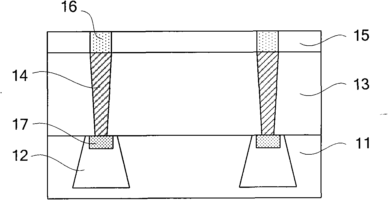
[0063] reference Figure 7A , First provide a wafer; the wafer includes: a semiconductor substrate 41 formed with an active region 42; a first dielectric layer 43 on the semiconductor substrate 41; penetrating the first dielectric layer 43 and interacting with the A contact plug 44 electrically connected to the source region 42; a second dielectric layer 45 formed on the first dielectric layer 43; and a second dielectric layer 45 penetrating through the second dielectric layer 45 and electrically connected to the contact plug 44 The metal layer 46.

[0064] In order to reduce the contact resistance, the wafer may also include a doped region 47 formed in the active region 42. The contact plug 44 is partially located in the active region 42 and passes through the doped region 47 and the doped region 47. The active region 42 is electrically connected, wherein the doped region 47 can be formed by ion implantation.

[0065] reference Figure 7B , The metal layer 46 and the second diele...


PUM

PropertyMeasurementUnit
Thicknessaaaaaaaaaa

Abstract

The invention provides a method for detecting the bottom outline of a contact plug, comprising the following steps of: providing a wafer, wherein the wafer comprises a semiconductor substrate with an active region, a first dielectric layer on the semiconductor substrate, the contact plug passing through the first dielectric layer and electrically connected with the active region, a second dielectric layer formed on the first dielectric layer and the contact plug, and a metal layer passing through the second dielectric layer and electrically connected with the contact plug; removing the metal layer and the second dielectric layer; removing a part of the first dielectric layer in a manner of dry etching; removing the contact plug so as to form a detection sample wafer; and using a scanning electron microscope to detect the detection sample wafer. In the invention, a clear picture of the bottom outline of the contact plug can be obtained by using the scanning electron microscope, and a precise detection result is obtained.

Description

Technical field [0001] The invention relates to the field of integrated circuit manufacturing, in particular to a method for detecting the bottom contour of a contact plug. Background technique [0002] With the rapid development of the information industry, the demand for processing a large amount of information has increased. Therefore, the demand for information storage media that can store a large amount of information has also increased, and the manufacturing process of the contact plug of the storage device has also been proposed higher and higher. The profile and Critical Dimension (CD) of the contact plug must meet the requirements accurately, otherwise the contact resistance (Rc) will be abnormal, which will affect the yield of the product. [0003] In order to ensure that the contact resistance of the semiconductor device meets the requirements, the industry often uses a transmission electron microscope (Transmission Electron Microscopy, TEM) to detect the manufactured co...

Claims


Application Information

Patent Timeline
IPC IPC(8): H01L21/66H01L21/768
Inventor 黄雪青林岱庆何永谢振
Owner WUHAN XINXIN SEMICON MFG CO LTD
Why Eureka
Try Eureka