A method for forming a double damascene structure

A metal structure and buffer layer technology, which is applied in semiconductor/solid-state device components, semiconductor devices, electrical components, etc., can solve the problems of many etching by-products in the double damascene process and poor morphology of the double damascene structure

Active Publication Date: 2020-10-27
SHANGHAI HUALI MICROELECTRONICS CORP
View PDF2 Cites 0 Cited by
  • Summary
  • Abstract
  • Description
  • Claims
  • Application Information

AI Technical Summary

Problems solved by technology

[0004] The purpose of the present invention is to provide a method for forming a double damascene structure, to solve the problems of the double damascene process etching by-products in the prior art and the poor appearance of the double damascene structure

Method used


Image

  • A method for forming a double damascene structure
  • A method for forming a double damascene structure
  • A method for forming a double damascene structure

Examples


Embodiment Construction

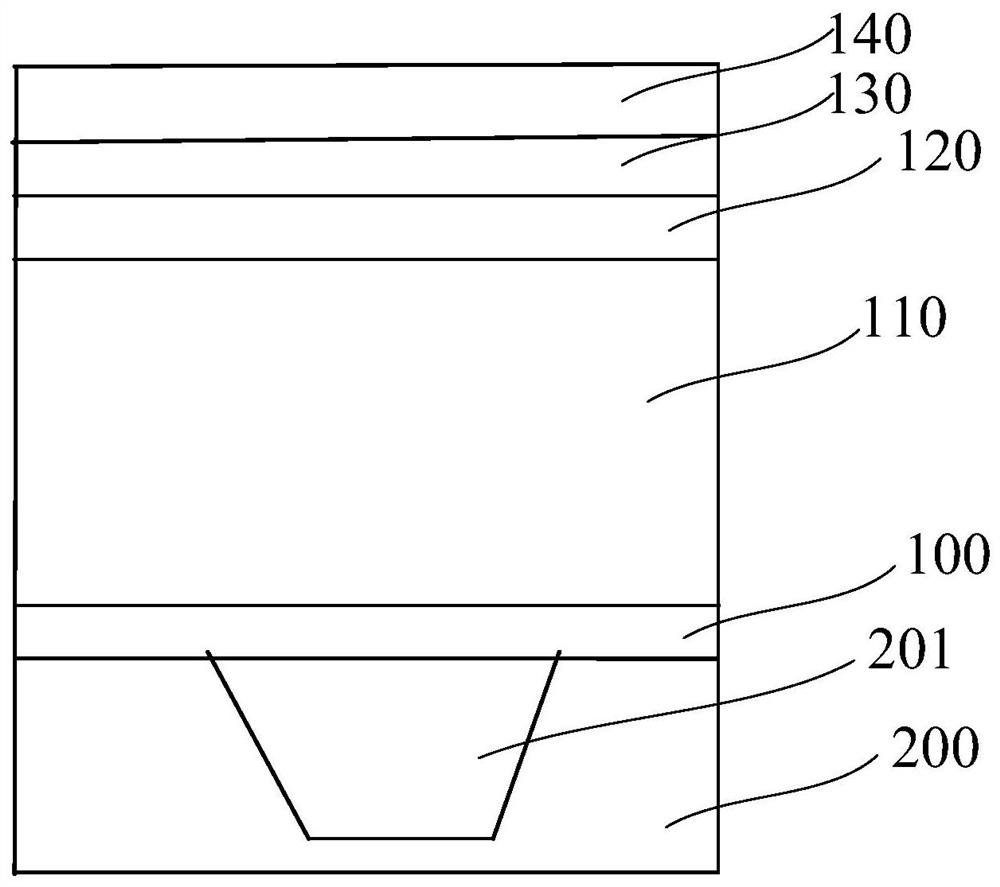
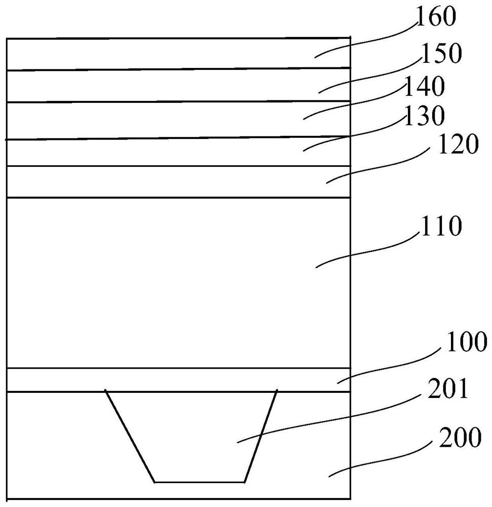
[0035] The method for forming a double damascene structure proposed by the present invention will be described in further detail below in conjunction with the accompanying drawings and specific embodiments. Advantages and features of the present invention will be apparent from the following description and claims. It should be noted that all the drawings are in a very simplified form and use imprecise scales, and are only used to facilitate and clearly assist the purpose of illustrating the embodiments of the present invention. In addition, the structures shown in the drawings are often a part of the actual structures. In particular, each drawing needs to display different emphases, and sometimes uses different scales.

[0036] The invention provides a method for forming a double damascene structure, referring to figure 1 , figure 1 It is a flow chart of a method for forming a double damascene structure according to an embodiment of the present invention, and the steps of t...


PUM

PropertyMeasurementUnit
heightaaaaaaaaaa
heightaaaaaaaaaa

Abstract

The present invention provides a method for forming a dual-damascene structure. The method comprises successively forming a barrier layer, a low dielectric constant layer, a first buffer layer, a hardmask layer, and a second buffer layer on the surface of a semiconductor structure in which a metal structure is embedded; etching the second buffer layer and the hard mask layer to form a first trench; etching the first buffer layer and the low dielectric constant layer to form a first via hole; downwards etching the low dielectric constant layer to form a second via hole; integrally etching thefirst via hole and the second via hole to form a second trench; opening the barrier layer to expose the metal structure so as to form the dual-damascene structure. Performing local via hole etching twice can well solve a load effect caused by etching and improve the dual-damascene etching defect, thereby improving the dual-damascene shape. Further, the second trench formed by the integral etchingis favorable for subsequent copper filling, which improves the reliability of the dual-damascene structure.

Description

technical field [0001] The invention relates to the technical field of semiconductor manufacturing, in particular to a method for forming a double damascene structure. Background technique [0002] With the rapid development of integrated circuits, the application range of integrated circuit chips has expanded rapidly. Due to different requirements, chip circuit design has become more and more complex, and the key dimensions have become smaller and smaller. relatively high requirements. [0003] During the dual damascene etching process, some areas contact the bottom copper prematurely, which is easy to cause the etching loading effect, and the etching by-products increase sharply, which will bring inevitable defects to the double damascene structure morphology, and even affect the final double damascene structure. Morphology of the Damascus structure. Contents of the invention [0004] The object of the present invention is to provide a method for forming a double damas...

Claims


Application Information

Patent Timeline
Patent Type & Authority Patents(China)
IPC IPC(8): H01L21/768H01L23/522H01L23/528
CPCH01L21/76807H01L21/76813H01L23/5226H01L23/528H01L23/5283
Inventor 贺可强周利民杨啸乔夫龙
Owner SHANGHAI HUALI MICROELECTRONICS CORP
Why Eureka
Try Eureka