Memory element and manufacturing method thereof

A memory element and manufacturing method technology, applied in semiconductor/solid-state device manufacturing, electrical components, electrical solid-state devices, etc., can solve the problems affecting the storage capacity and process yield of vertical-channel three-dimensional NAND flash memory components, memory cell defects, affecting components storage capacity, etc.

Active Publication Date: 2016-10-05
MACRONIX INT CO LTD
View PDF7 Cites 11 Cited by
  • Summary
  • Abstract
  • Description
  • Claims
  • Application Information

AI Technical Summary

Problems solved by technology

The setting of the etched channel will occupy the formation space of the memory cell and affect the storage capacity of the element
In addition, the sacrificial layer is easy to remain in the multi-layer stack stru

Method used


Image

  • Memory element and manufacturing method thereof
  • Memory element and manufacturing method thereof
  • Memory element and manufacturing method thereof

Examples


Example Embodiment

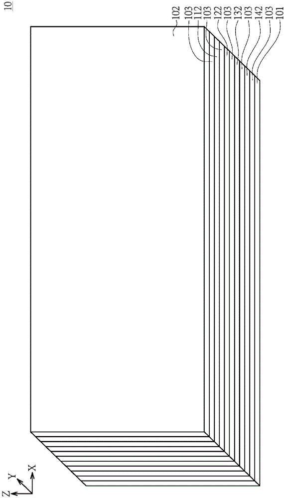
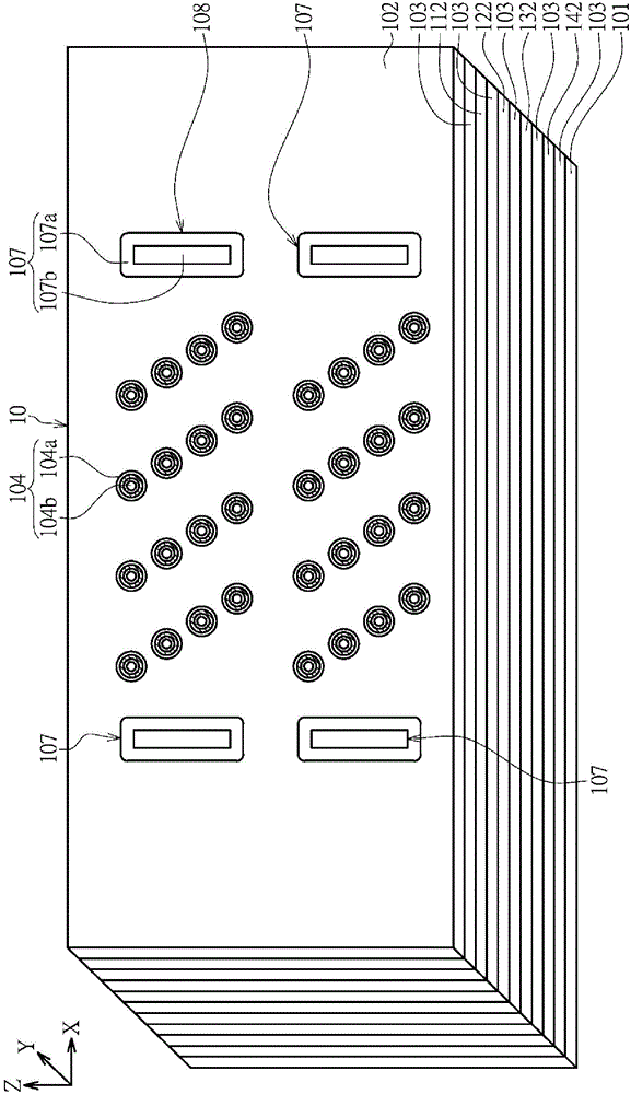
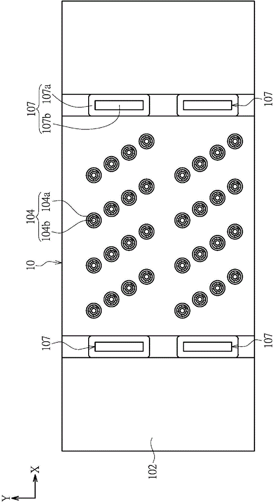
[0047] The present invention provides a memory element and a manufacturing method thereof, which can reduce the overall resistivity of the memory element to reduce signal transmission delay caused by resistance and capacitance. In order to make the above-mentioned embodiments and other objectives, features and advantages of the present invention more comprehensible, a vertical channel type three-dimensional NAND flash memory device 100 is specifically cited below as a preferred embodiment, and will be described in detail with the accompanying drawings.

[0048] However, it must be noted that these specific implementation cases and methods are not intended to limit the present invention. The present invention can still be implemented using other features, elements, methods and parameters. The preferred embodiments are only used to illustrate the technical features of the present invention, and not to limit the scope of the claims of the present invention. Those with ordinary know...


PUM


Abstract

The invention discloses a memory element and a manufacturing method thereof. The memory element comprises a plurality of silicon-containing conductive layers and the plurality of silicon-containing conductive layers are parallel to each other and vertically stacked on the substrate. A plurality of serial selection lines are located over the silicon-containing conductive layers and are extending along a first direction. A plurality of serial lines are vertical to the silicon-containing conductive layers and the serial selection lines, and are electrically connected to the serial selection lines. A plurality of bit lines are located at the serial selection lines and are extending along a second direction. Multi-set and multi-layer plug structures are arranged along the first direction to respectively sandwich the plurality of serial lines between every two adjacent multi-layer plug structures. Each multi-layer plug structure is composed of a plurality of via plugs and each via plug is correspondingly connected with one silicon-containing conductive layer. The memory element further comprises a plurality of metal word lines. Each metal word line extends along the first direction and is electrically connected with one via plug connected with the same silicon-containing conductive layer.

Description

technical field [0001] The present invention relates to a semiconductor element and its manufacturing method, and in particular to a memory element and its manufacturing method. Background technique [0002] Non-volatile memory devices, such as flash memory, have the property of not losing information stored in memory cells when power is removed. It has been widely used in solid-state mass storage applications for portable music players, mobile phones, digital cameras, etc. In order to meet the demand for higher density storage capacity, there are currently various three-dimensional memory devices with different structures, such as single-gate memory cells, double-gate memory cells, and wraparound gate memory cells. A three-dimensional flash memory element of a surrounding gate memory cell is proposed. [0003] Three-dimensional memory elements, such as vertical-channel (VC) three-dimensional NAND flash memory elements, have many layers of stacked layers (memory layers) st...

Claims


Application Information

Patent Timeline
IPC IPC(8): H01L27/115H01L29/43H01L23/535H01L21/8247H01L21/768H01L21/28
Inventor 陈士弘
Owner MACRONIX INT CO LTD
Why Eureka
Try Eureka