Flash memory and its programming method

A programming method and memory technology, applied in the direction of static memory, read-only memory, digital memory information, etc., can solve the problem that the storage unit is not necessarily uniform, achieve the effect of realizing the threshold distribution range and improving the data retention characteristics

Active Publication Date: 2019-08-27
WINBOND ELECTRONICS CORP
View PDF6 Cites 0 Cited by
  • Summary
  • Abstract
  • Description
  • Claims
  • Application Information

AI Technical Summary

Problems solved by technology

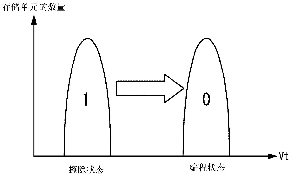
[0004] In the tunnel oxide film or floating gate of the memory cell, there may be variations due to factors such as fluctuations in manufacturing process parameters or changes over time, so all memory cells may not be uniform.

Method used


Image

  • Flash memory and its programming method
  • Flash memory and its programming method
  • Flash memory and its programming method

Examples


Embodiment Construction

[0107] Hereinafter, embodiments of the present invention will be described in detail with reference to the drawings. In addition, it should be noted that in the drawings, each part is emphasized for easy understanding, and the scale of the actual device (device) is not the same.

[0108] Figure 6 It is a block diagram of the overall structure of the NAND flash memory according to an embodiment of the present invention. Such as Figure 6As shown, the flash memory 100 includes: a memory array 110, formed with a plurality of memory cells arranged in rows and columns; an input / output buffer (buffer) 120, connected to an external input / output terminal I / O; an address register 130, Receive address data from the input / output buffer 120; cache memory (cache memory) 140 keeps the input / output data; controller 150 generates control signals C1, C2, C3, etc., the control signals C1, C2, C3 etc. are based on the command data (command data) from the input / output buffer 120 and external ...


PUM


Abstract

The invention provides a flash memory and a programming method thereof. A programming method for a flash memory includes: verifying and reading, after applying a programming voltage to a selected word line, verifying whether the threshold of the selected memory cell is qualified, and verifying and reading includes the steps of precharging the voltage to the bit line, using The step in which the voltage of the precharged bit line can be discharged to the source line and the step in which the voltage of the bit line is read out after the discharge step, for the discharge period from the start of discharge of the bit line to the start of readout, the initial programming The discharge period for verify read after voltage application is set to be longer than the discharge period for verify read after program voltage application thereafter. The programming method of the flash memory provided by the present invention can realize the narrowing of the threshold value distribution range.

Description

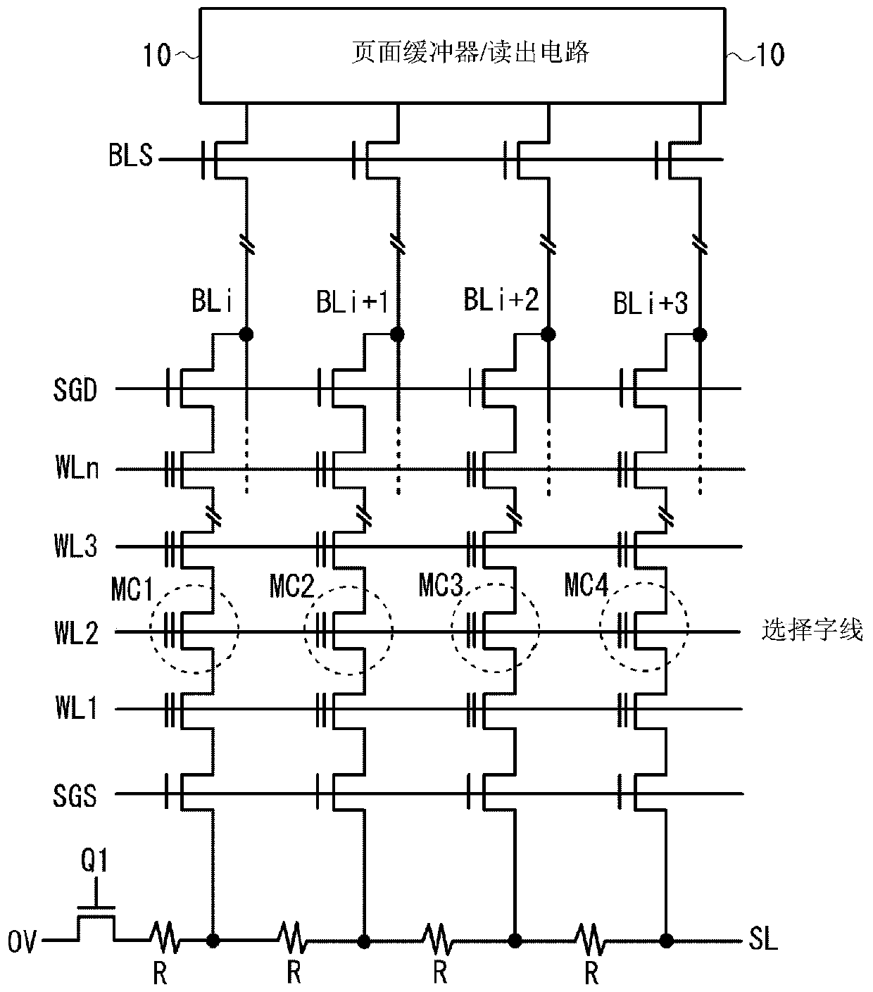
technical field [0001] The invention relates to a non-volatile semiconductor storage device such as a NAND flash memory (flash memory), in particular to a flash memory and a programming method thereof. Background technique [0002] The NAND type flash memory includes a plurality of NAND strings (string), and one NAND string has: a plurality of memory cells (memory cells) connected in series; a source line side selection transistor connected to one end of the memory cells; and A bit line side select transistor connected to the other end of the memory cell. The control gate of each memory cell is connected to the corresponding word line, the select gate line SGS is connected to the gate of the select transistor on the source line side, and the select gate line SGD is connected to the gate of the select transistor on the bit line side. A plurality of these NAND strings are formed along the row direction in the P well, and one P well constitutes one block of the memory cell arr...

Claims


Application Information

Patent Timeline
Patent Type & Authority Patents(China)
IPC IPC(8): G11C16/10G11C16/34
CPCG11C7/12G11C16/0483G11C16/10G11C16/24G11C16/26G11C16/32G11C16/3459
Inventor 白田里一郎
Owner WINBOND ELECTRONICS CORP
Why Eureka
Try Eureka