A kind of manufacturing method of flash memory

A manufacturing method and memory technology, applied in semiconductor devices, electrical solid state devices, electrical components, etc., can solve the problems of reducing the data retention characteristics of flash memory, and the difficulty in guaranteeing the performance of tunnel oxides and pad oxides, etc., to achieve improved Effects of the data retention feature

Active Publication Date: 2018-06-19
GIGADEVICE SEMICON SHANGHAI INC +1
View PDF5 Cites 0 Cited by
  • Summary
  • Abstract
  • Description
  • Claims
  • Application Information

AI Technical Summary

Problems solved by technology

[0003] In flash memory, data retention performance (Data Retention) is an important performance index. In order to improve data retention performance, in-situ steam generation (In-Situ Steam Generation, referred to as ISSG) is generally used in the prior art on the channel boundary The purpose of forming a pad oxide is to make the corner of the channel boundary rounded (cornerrounding) to ensure the thickness and insulation performance of the tunnel oxide at the edge of the channel, and to prevent the tip discharge from causing breakdown or performance damage to the flash memory device. However, due to the influence of the isolation oxide in the subsequent process, it is difficult to guarantee the performance of the tunnel oxide and pad oxide, thereby reducing the data retention characteristics of the flash memory

Method used


Image

  • A kind of manufacturing method of flash memory
  • A kind of manufacturing method of flash memory
  • A kind of manufacturing method of flash memory

Examples


Embodiment Construction

[0039] The present invention will be further described in detail below in conjunction with the accompanying drawings and embodiments. It should be understood that the specific embodiments described here are only used to explain the present invention, but not to limit the present invention. In addition, it should be noted that, for the convenience of description, only parts related to the present invention are shown in the drawings but not all content.

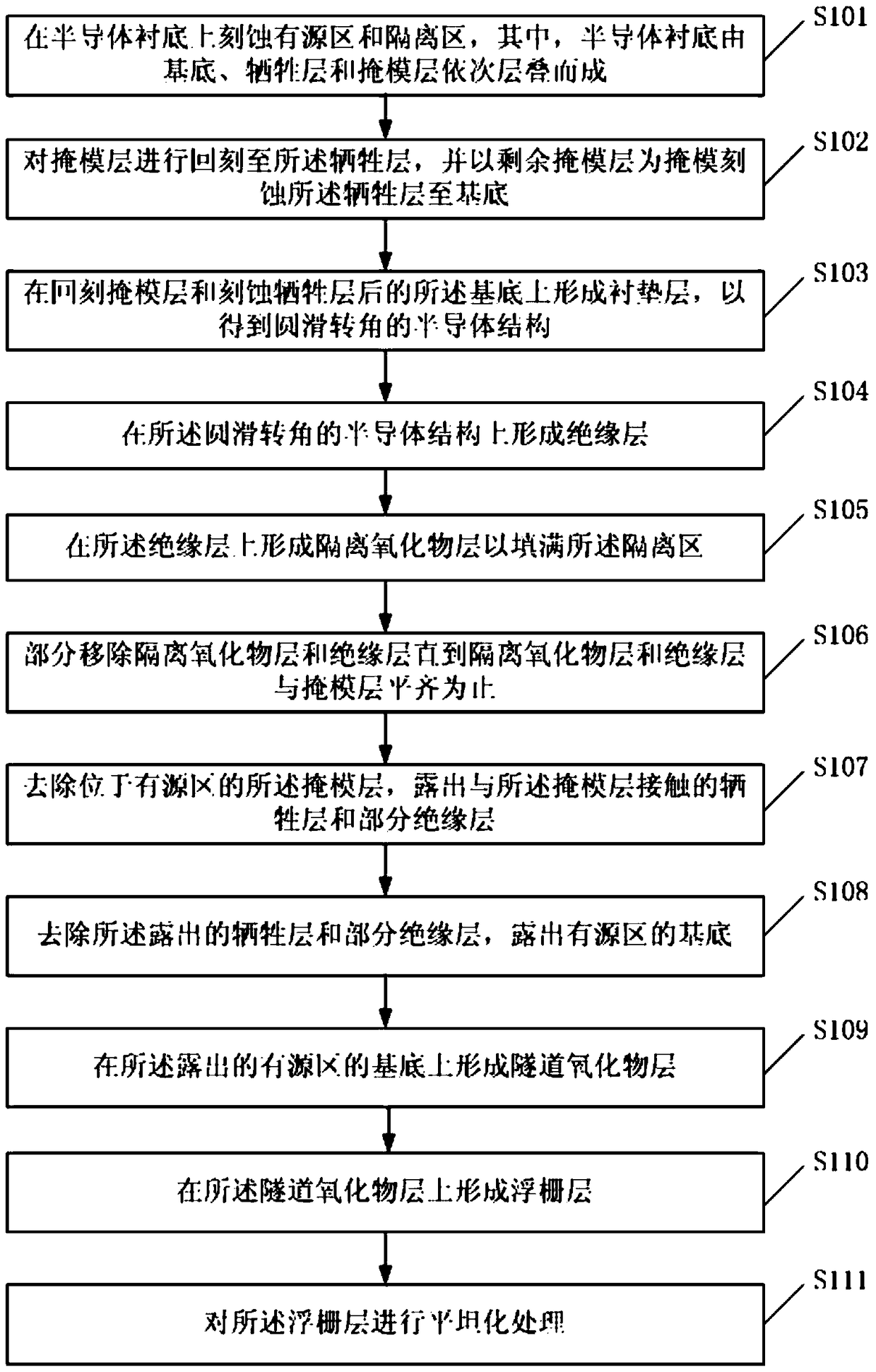
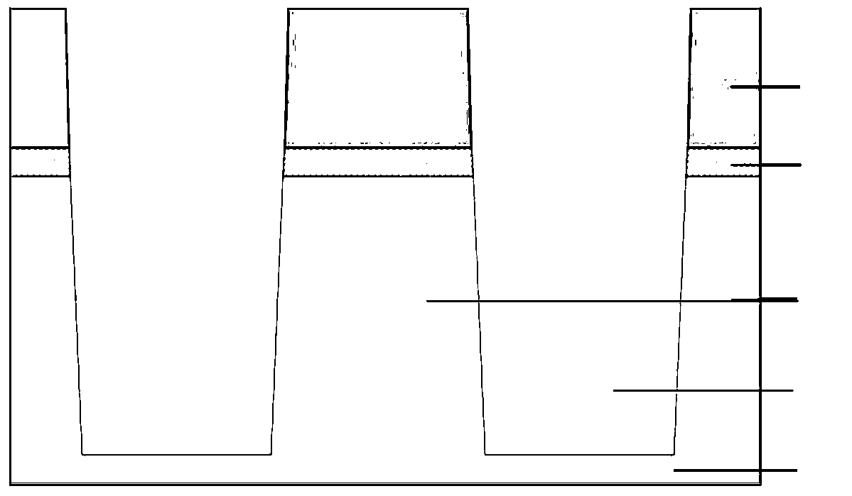
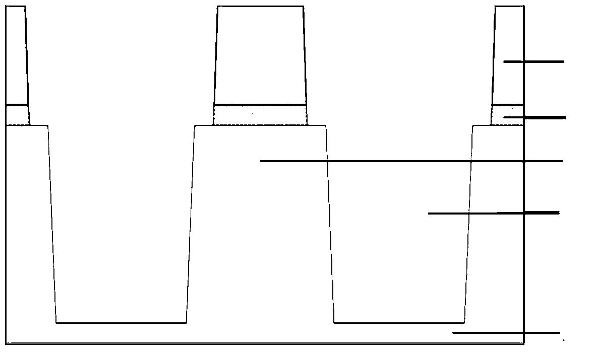
[0040] figure 1 is a flow chart of a method for manufacturing a flash memory provided by an embodiment of the present invention, such as figure 1 As shown, the flash memory made by the manufacturing method of the flash memory can be used in mobile devices such as notebook computers, cameras and mobile phones, such as figure 1 As shown, the manufacturing method of the flash memory includes:

[0041] Step S101 , etching an active region and an isolation region on a semiconductor substrate, wherein the semiconductor substrate i...


PUM


Abstract

The invention discloses a method for manufacturing a flash memory, which comprises etching an active region and an isolation region on a semiconductor substrate, wherein the semiconductor substrate is formed by stacking a substrate, a sacrificial layer and a mask layer in sequence, and the mask is etched back after the semiconductor substrate is sequentially stacked. A liner layer is formed on the substrate after the sacrificial layer is etched to obtain a semiconductor structure with rounded corners, an insulating layer is formed on the semiconductor structure with rounded corners, an isolation oxide layer is formed on the insulating layer to fill the isolation region, and part of Remove the isolation oxide layer and insulating layer until the isolation oxide layer and the insulating layer are flush with the mask layer, remove the mask layer located in the active area, expose the sacrificial layer and part of the insulating layer in contact with the mask layer, remove The exposed sacrificial layer and part of the insulating layer expose the substrate of the active region, and a tunnel oxide layer and a floating gate layer are sequentially formed on the exposed substrate of the active region. The present invention can prevent the isolation oxide of the isolation region from affecting the tunnel oxide and the pad layer, thereby improving the data retention characteristics of the flash memory.

Description

technical field [0001] The invention relates to the field of semiconductor manufacturing, in particular to a method for manufacturing a flash memory. Background technique [0002] Flash memory is not easy to lose and can be repeatedly erased and read and written. In addition, it also has the characteristics of fast transmission speed and low power consumption, which makes flash memory widely used in portable products, information, communication and consumer electronics products. . [0003] In flash memory, data retention performance (Data Retention) is an important performance index. In order to improve data retention performance, in-situ steam generation (In-Situ Steam Generation, referred to as ISSG) is generally used in the prior art on the channel boundary The purpose of forming a pad oxide is to make the corner of the channel boundary rounded (cornerrounding) to ensure the thickness and insulation performance of the tunnel oxide at the edge of the channel, and to preve...

Claims


Application Information

Patent Timeline
Patent Type & Authority Patents(China)
IPC IPC(8): H01L27/11524
Inventor 于法波舒清明
Owner GIGADEVICE SEMICON SHANGHAI INC
Why Eureka
Try Eureka