Substrate, manufacture method thereof, and electronic device
A manufacturing method and substrate technology, applied in the direction of electrical solid devices, electrical components, semiconductor devices, etc., can solve problems such as inability to cut and repair, welding of signal lines, etc., and achieve the effect of improving the repair rate and reducing production costs
- Summary
- Abstract
- Description
- Claims
- Application Information
AI Technical Summary
Problems solved by technology
Method used
Image

Examples
Embodiment 1
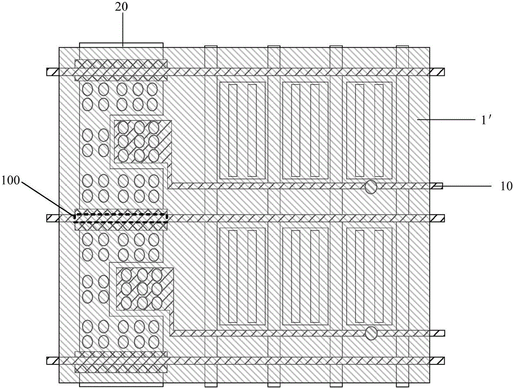
[0029] combine figure 2 and image 3 As shown, the substrate in this embodiment includes at least two insulated signal lines, and at least two of the signal lines are intersected, and a signal line overlapping region 100 is formed at the intersection. It should be noted that, usually, an insulating layer is provided between signal lines of different layers to realize insulation. The intersection here refers to the intersection of the orthographic projection of the signal lines on the plane where the substrate is located, and the overlapping area of the signal lines corresponds to the intersection area of the orthographic projection of the signal lines on the plane where the substrate is located.
[0030] The substrate also includes a first area, the signal line includes a first signal line 20 located in the first area, the substrate also includes an electrode line 10, and a jumper 1 is provided to electrically connect the electrode line 10 and the first signal line 20. ...
Embodiment 2
[0058] For ease of description and understanding, in this embodiment, the technical solution of the present invention is also described in detail by taking the thin film transistor array substrate as an example.
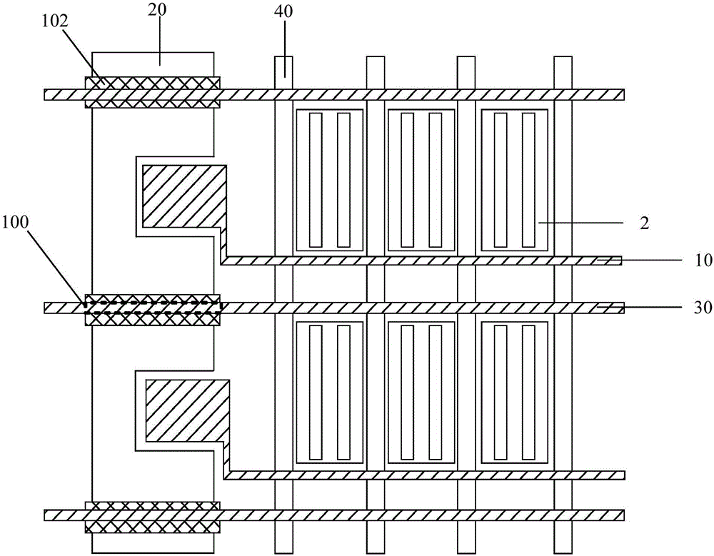
[0059] In the first embodiment, jumpers are set to include the first substructure located in the non-display area (that is, the first area), and a certain distance is separated between two adjacent first substructures, and the signal line overlapping area is located in the adjacent Between the two first substructures, a part of the isolation area is located in the area between the signal line overlapping area and the corresponding first substructure, that is, neither the signal line overlapping area nor the isolation area is laid Jumper, so that when the electrostatic breakdown occurs in the overlapping area of the signal line, laser cutting repair can be performed in the partition area, which overcomes the problem that the jumper is easy to weld with the signal lin...
Embodiment 3
[0066] In the above two embodiments, jumpers are not laid in the signal line overlapping area, that is, neither the signal line overlapping area nor the partition area around the signal line overlapping area is laid with signal lines, so that when the signal lines overlap When electrostatic breakdown occurs in the overlapping area, laser cutting repair can be performed in the partition area, so as to overcome the problem that the jumper wire is easily fused with the signal line and cannot be repaired.
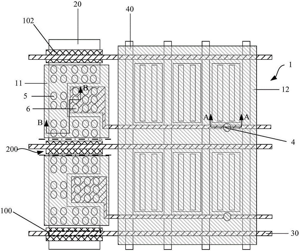
[0067] The difference from the above two embodiments is that the combination Figure 8-Figure 10 As shown, in this embodiment, jumpers are laid on the signal line overlapping area 100 of the substrate, and jumpers are not laid on the isolation area 200 around the signal line overlapping area 100 .
[0068] Then, the jumper 1 in this embodiment includes a third substructure 15 and a fourth substructure 16 , the third substructure 15 is laid on the periphery of the isolation area...
PUM
 Abstract
Description
Claims
Application Information
 - R&D
- Intellectual Property
- Life Sciences
- Materials
- Tech Scout
- Unparalleled Data Quality
- Higher Quality Content
- 60% Fewer Hallucinations
Browse by: Latest US Patents, China's latest patents, Technical Efficacy Thesaurus, Application Domain, Technology Topic, Popular Technical Reports.
© 2025 PatSnap. All rights reserved.Legal|Privacy policy|Modern Slavery Act Transparency Statement|Sitemap|About US| Contact US: help@patsnap.com