Array substrate, manufacturing method of array substrate, display panel and display device

An array substrate and substrate technology, applied in semiconductor/solid-state device manufacturing, static indicators, instruments, etc., can solve problems such as electrostatic accumulation and electrostatic breakdown

Inactive Publication Date: 2016-11-30
BOE TECH GRP CO LTD +1
View PDF5 Cites 2 Cited by
  • Summary
  • Abstract
  • Description
  • Claims
  • Application Information

AI Technical Summary

Problems solved by technology

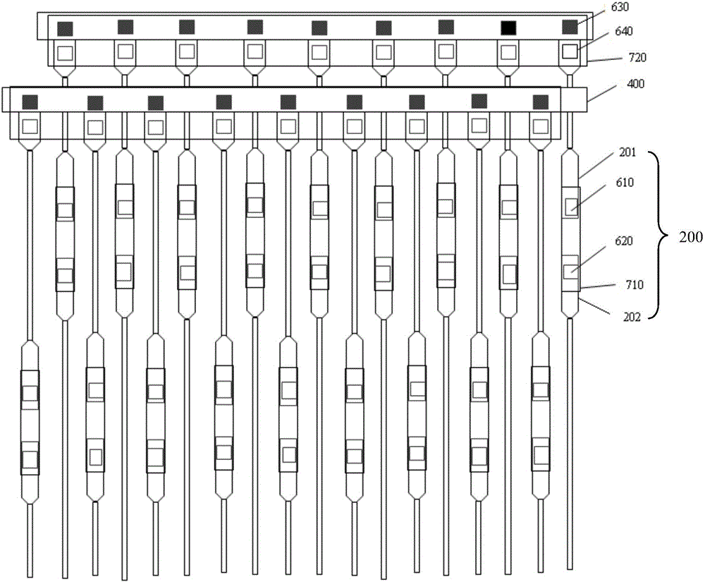
Although an insulating layer is formed between these traces, because the longer traces tend to cause static electricity to accumulate, this will cause electrostatic breakdown (ESD) in the area where the projections of the traces on the substrate overlap in the subsequent process.

Method used


Image

  • Array substrate, manufacturing method of array substrate, display panel and display device
  • Array substrate, manufacturing method of array substrate, display panel and display device
  • Array substrate, manufacturing method of array substrate, display panel and display device

Examples


Embodiment Construction

[0033] In order to make the purpose, technical solutions and advantages of the embodiments of the present invention clearer, the embodiments of the present invention will be described in detail below with reference to the accompanying drawings. Apparently, the described embodiments are only some of the embodiments of the present invention, but not all of them.

[0034] Throughout this specification, reference to features, advantages, or similar language, does not imply that all of the features and advantages that can be achieved with the invention should be or are in any single embodiment of the invention. Rather, words referring to the features and advantages are understood to mean that a specific feature, advantage, or characteristic described in connection with an embodiment is included in at least one embodiment of the invention. Thus, discussions of the features and advantages, and similar language, throughout this specification may, but do not necessarily, refer to the s...


PUM


Abstract

The invention relates to an array substrate, a manufacturing method of the array substrate, a display panel and a display device. The array substrate comprises a substrate, first leads, a first insulation layer, second leads and a connection part, wherein the first leads are positioned on the substrate; the first insulation layer is positioned on the first leads; the second leads are positioned on the first insulation layer; at least parts of projections of the first leads and the second leads on the substrate are overlapped; at least one of the first leads and the second leads consists of conductive segments which are arranged at intervals; and the connection part is used for electrically connecting adjacent conductive segments of the first leads or the second leads.

Description

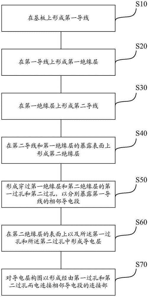
technical field [0001] Embodiments of the present invention relate to an array substrate and a manufacturing method thereof, a display panel and a display device. Background technique [0002] In the structure of the array substrate, no matter in the display area or in the peripheral area such as the test area (shorting bar), the projection of the wiring on the substrate such as the gate layer wiring and the source-drain electrode layer wiring is at least partially overlapping. Although an insulating layer is formed between these traces, the longer traces tend to cause static electricity to accumulate, which will cause electrostatic breakdown (ESD) in the area where the projections of the traces on the substrate overlap in subsequent processes. Contents of the invention [0003] According to one aspect of the present invention, an array substrate is provided, comprising: a substrate; a first wire located on the substrate; a first insulating layer located on the first wire...

Claims


Application Information

Patent Timeline
Patent Type & Authority Applications(China)
IPC IPC(8): H01L27/12H01L21/77
CPCH01L27/124H01L27/1259H01L27/0288H01L27/1262G09G3/006H01L27/0292H01L22/32H01L27/1222
Inventor 刘成伟张心杰
Owner BOE TECH GRP CO LTD
Why Eureka
Try Eureka