Multiple circuit board for liquid crystal display panels and method for manufacturing liquid crystal display panels

a liquid crystal display panel and multi-circuit board technology, applied in the manufacture of electrode systems, electric discharge tubes/lamps, instruments, etc., can solve the problems of not taking special effective measures for scanning lines, and no specific information on electrostatic breakdown of circuit elements connected to scanning lines, so as to prevent electrostatic breakdown of circuit elements

Active Publication Date: 2014-12-11
JAPAN DISPLAY INC
View PDF0 Cites 2 Cited by
  • Summary
  • Abstract
  • Description
  • Claims
  • Application Information

AI Technical Summary

Benefits of technology

[0008]An object of the invention is to prevent electrostatic breakdown of circuit elements connected to scanning lines.
[0009](1) A multiple circuit board according to the invention is a multiple circuit board for cutting into a plurality of array boards used for a plurality of liquid crystal display panels, including a board having a plurality of product regions respectively corresponding to the plurality of array boards and an out-of-product region, out-of-product wires provided in the out-of-product region, waveform wires electrically connected to the out-of-product wires and extending to depict waveforms to alternately pass inside and outside of the respective product regions, circuit elements provided in respective display regions of the plurality of product regions, scanning circuits provided adjacent to the respective display regions of the plurality of product regions, and a plurality of scanning lines extending from the scanning circuits to both sides in each of the product regions and connecting to the circuit elements at one side and connecting to the waveform wires inside the product region at the other side. According to the invention, the scanning lines are connected to the out-of-product wires via the waveform wires, and static electricity may be transferred to the out-of-product wires. Thereby, electrostatic breakdown of the circuit elements may be prevented. Further, the waveform wires have shapes depicting waveforms, and may be cut along the straight lines into pieces. Therefore, the plurality of scanning lines electrically conducting to each other through connection to the waveform wires maybe electrically separated by one cutting process.
[0017](9) A method for manufacturing liquid crystal display panels according to the invention includes preparing a multiple circuit board having a board having a plurality of product regions and an out-of-product region used for a plurality of liquid crystal display panels, out-of-product wires provided in the out-of-product region, waveform wires electrically connected to the out-of-product wires and extending to depict waveforms to alternately pass ends of the adjacent product regions, circuit elements provided in respective display regions of the plurality of product regions, scanning circuits provided adjacent to the respective display regions of the plurality of product regions, and a plurality of scanning lines extending from the scanning circuits to both sides in each of the product regions and connecting to the circuit elements at one side and connecting to the waveform wires inside the product region at the other side, and cutting the multiple circuit board in correspondence with the plurality of product regions, wherein cutting the multiple circuit board includes separating the adjacent product regions in which the waveform wires alternately pass along one cut line, the one cut line passes a location to separate the waveform depicted by the waveform wires into two half waveforms in which a plurality of convex parts are alternately arranged at opposite sides to each other with gaps, and the plurality of scanning lines are connected to the waveform wires at the convex sides. According to the invention, only by separating the adjacent product regions along one cut line, the waveform wires may be separated with respect to each convex part. Therefore, the plurality of scanning lines electrically conducting to each other through connection to the waveform wires may be electrically separated by one cutting process. Further, the scanning lines are connected to the out-of-product wires via the waveform wires, and static electricity may be transferred to the out-of-product wires. Thereby, electrostatic breakdown of the circuit elements may be prevented.

Problems solved by technology

In related art, as measures for electrostatic breakdown, data lines are connected to a protection circuit and a control signal line of a scanning circuit is connected to a common line outside of the product, however, any particularly effective measures have not been taken for scanning lines.
However, no measures for electrostatic breakdown of circuit elements connected to scanning lines have been specifically disclosed.

Method used


Image

  • Multiple circuit board for liquid crystal display panels and method for manufacturing liquid crystal display panels
  • Multiple circuit board for liquid crystal display panels and method for manufacturing liquid crystal display panels
  • Multiple circuit board for liquid crystal display panels and method for manufacturing liquid crystal display panels

Examples


Embodiment Construction

[0026]As below, embodiments of the invention will be explained with reference to the drawings.

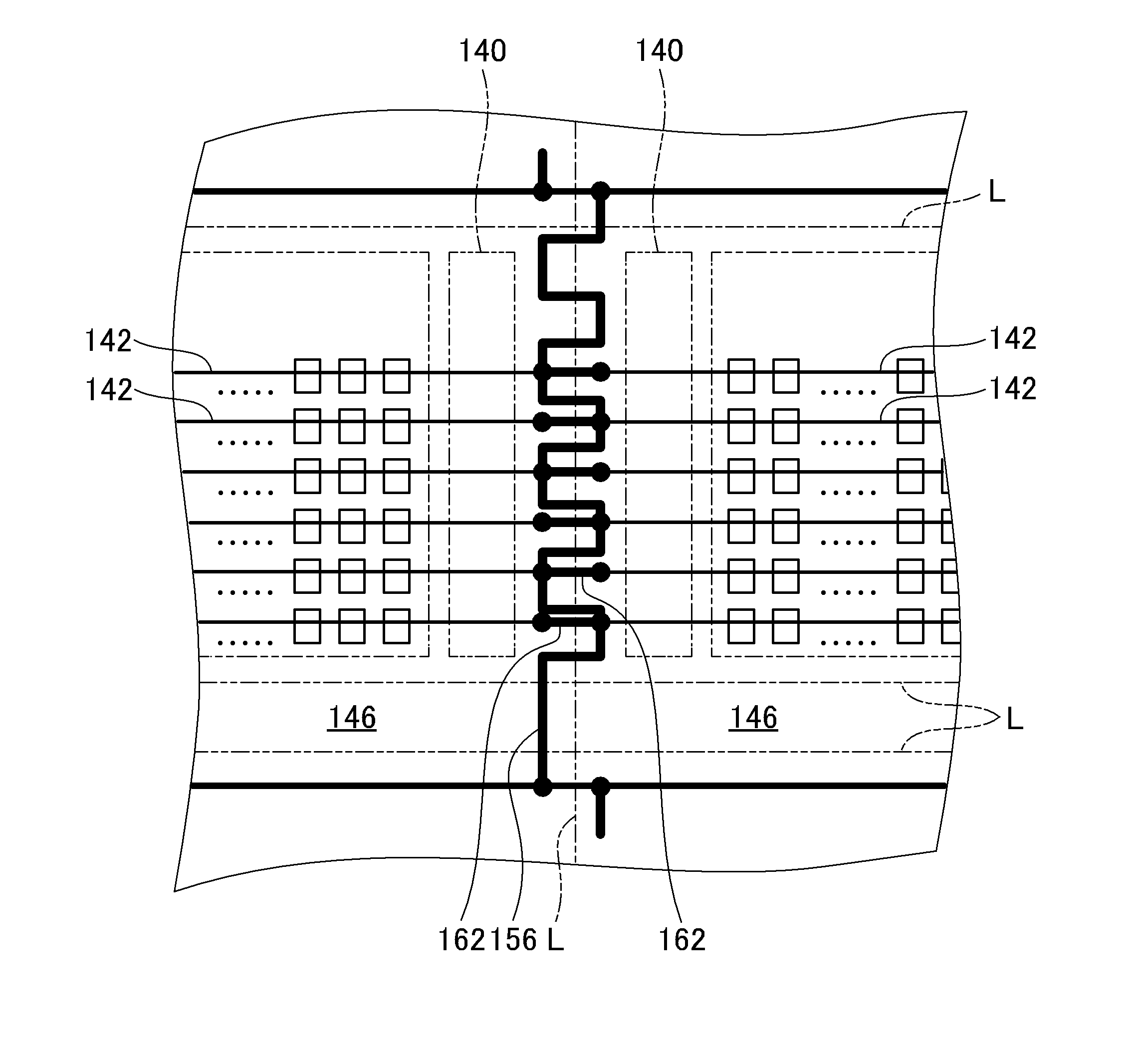
[0027]FIG. 1 is a sectional view showing a liquid crystal display panel. The liquid crystal display panel has a color filter board 10. The color filter board 10 includes a black matrix 12, a color filter layer 14, a planarizing layer 16, and a first alignment film 18. A second alignment film 20 is provided to be opposed to the first alignment film 18 with a cell gap in between. A liquid crystal material 22 is provided between the first alignment film 18 and the second alignment film 20.

[0028]An array board 24 is provided to be opposed to the color filter board 10. The array board 24 includes a circuit layer 26. A circuit for driving the liquid crystal material 22 is formed in the circuit layer 26. The second alignment film 20 is formed on the circuit layer 26. As a modified example, a color filter layer may be formed on the array board 24 and, in this case, the array board 24 also serves as...


PUM

PropertyMeasurementUnit
electrostatic breakdownaaaaaaaaaa
shapesaaaaaaaaaa
electricallyaaaaaaaaaa

Abstract

A multiple circuit board includes a board having a plurality of product regions respectively corresponding to a plurality of array boards and an out-of-product region, out-of-product wires provided in the out-of-product region, waveform wires electrically connected to the out-of-product wires and extending to depict waveforms to alternately pass inside and outside of the respective product regions, circuit elements provided in respective display regions of the plurality of product regions, scanning circuits provided adjacent to the respective display regions of the plurality of product regions, and a plurality of scanning lines extending from the scanning circuits to both sides in each of the product regions and connecting to the circuit elements at one side and connecting to the waveform wires inside the product region at the other side.

Description

CROSS-REFERENCE TO RELATED APPLICATION[0001]The present application claims priority from Japanese application JP2013-120108 filed on Jun. 6, 2013, the content of which is hereby incorporated by reference into this application.BACKGROUND OF THE INVENTION[0002]1. Field of the Invention[0003]This invention relates to a multiple circuit board for liquid crystal display panels and a method for manufacturing liquid crystal display panels.[0004]2. Description of the Related Art[0005]Liquid crystal display panels are generally driven by a matrix system. In the matrix system, a plurality of data lines and a plurality of scanning lines extend in directions in which the lines intersect. When a scanning signal is input to the scanning line, the scanning line is selected, and signals of the data lines are applied to pixels corresponding to the selected scanning line.[0006]In related art, as measures for electrostatic breakdown, data lines are connected to a protection circuit and a control signa...

Claims


Application Information

Patent Timeline
Patent Type & Authority Applications(United States)
IPC IPC(8): G02F1/1362G02F1/1333
CPCG02F1/1333G02F1/136204G02F1/133351
Inventor AGATA, KENTARO
Owner JAPAN DISPLAY INC
Why Eureka
Try Eureka