Substrate liquid processing device and substrate liquid processing method

A technology for liquid processing and substrate processing, applied in semiconductor/solid-state device manufacturing, electrical components, circuits, etc., can solve problems such as electrostatic breakdown, and achieve the effect of preventing electrostatic breakdown

Active Publication Date: 2016-12-14
TOKYO ELECTRON LTD
View PDF7 Cites 1 Cited by
  • Summary
  • Abstract
  • Description
  • Claims
  • Application Information

AI Technical Summary

Problems solved by technology

[0004] In addition, when the substrate and structural parts are charged, electrostatic breakdown may occur on the circuit formation surface of the substrate (the surface on which electronic components such as transistors and diodes are formed, and the wiring connecting them, etc.) when the charge is discharged.

Method used


Image

  • Substrate liquid processing device and substrate liquid processing method
  • Substrate liquid processing device and substrate liquid processing method
  • Substrate liquid processing device and substrate liquid processing method

Examples


Embodiment Construction

[0041]The specific structure of the substrate liquid processing apparatus, the substrate liquid processing method used in the substrate liquid processing apparatus, and the substrate liquid processing program for causing the substrate liquid processing apparatus to perform liquid processing on a substrate according to the present invention will be described below with reference to the accompanying drawings. .

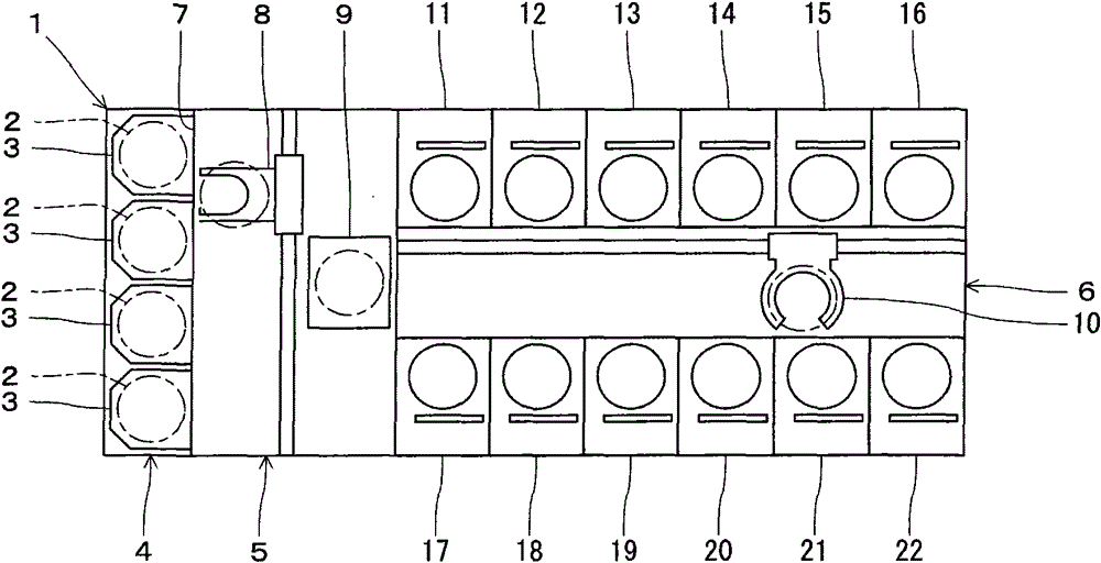
[0042] Such as figure 1 As shown, a substrate loading and unloading table 4 is formed at the front end of the substrate liquid processing apparatus 1, and the substrate loading and unloading table 4 collects a plurality of (for example, 25) substrates 2 (here, semiconductor wafers) on a carrier 3 to carry out loading and unloading. , and a substrate transport chamber 5 is formed at the rear of the substrate loading and unloading table 4. The substrate transport chamber 5 is used to transport the substrates 2 accommodated on the carrier 3 piece by piece. The substrate ...


PUM


Abstract

The invention provides a substrate liquid processing device and a substrate liquid processing method. Prevents electrostatic breakdown due to the discharge of charges carried by the substrate. In the present invention, in the substrate liquid processing device (1), the substrate liquid processing method, and the computer-readable recording medium (48) recording the substrate liquid processing program for performing liquid processing on the substrate (2), in Before the liquid treatment step of liquid-treating the circuit-forming surface of the substrate (2) with a substrate-treating liquid, a static-elimination treatment step is performed, in which the circuit-forming surface of the substrate (2) is formed using a static-elimination treatment liquid. The surface opposite to the surface is treated, thereby releasing the charges carried by the substrate (2).

Description

technical field [0001] The present invention relates to a substrate liquid processing device, a substrate liquid processing method, and a computer-readable recording medium recorded with a substrate liquid processing program for performing liquid processing on a substrate with a processing liquid. Background technique [0002] Conventionally, when manufacturing semiconductor components, flat panel displays, etc., substrates such as semiconductor wafers and liquid crystal substrates are cleaned and etched using processing liquids such as cleaning agents and etchant using substrate liquid processing equipment. [0003] In this substrate liquid processing device, due to various reasons such as charging of the processing liquid and friction of the movable part, the substrate processed by the substrate liquid processing device, components constituting the substrate liquid processing device, etc. may be charged due to static electricity. charge. [0004] In addition, when the sub...

Claims


Application Information

Patent Timeline
Patent Type & Authority Patents(China)
IPC IPC(8): H01L21/00H01L21/02
Inventor 田中裕司南辉臣川渕洋介伊藤规宏上村史洋薮田贵士小佐井一树乌野崇关口贤治藤井康
Owner TOKYO ELECTRON LTD
Why Eureka
Try Eureka