Terahertz graphene microstructure modulator

A microstructure and graphene technology, applied in instruments, nonlinear optics, optics, etc., can solve the problems of poor electronic control tunability and large loss

Inactive Publication Date: 2016-12-07
SHANGHAI NORMAL UNIVERSITY
View PDF2 Cites 18 Cited by
  • Summary
  • Abstract
  • Description
  • Claims
  • Application Information

AI Technical Summary

Problems solved by technology

[0009] The common constituent materials of metamaterials mainly include metals (such as Ag, Au) and semiconductors (such as

Method used


Image

  • Terahertz graphene microstructure modulator
  • Terahertz graphene microstructure modulator
  • Terahertz graphene microstructure modulator

Examples


Embodiment Construction

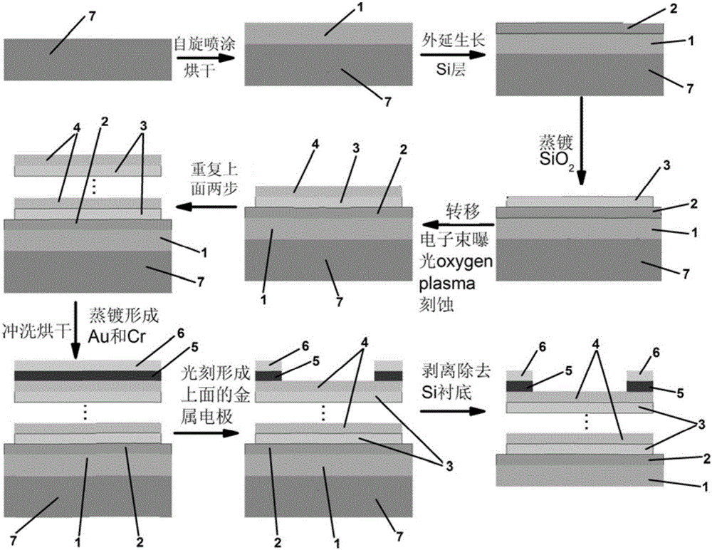
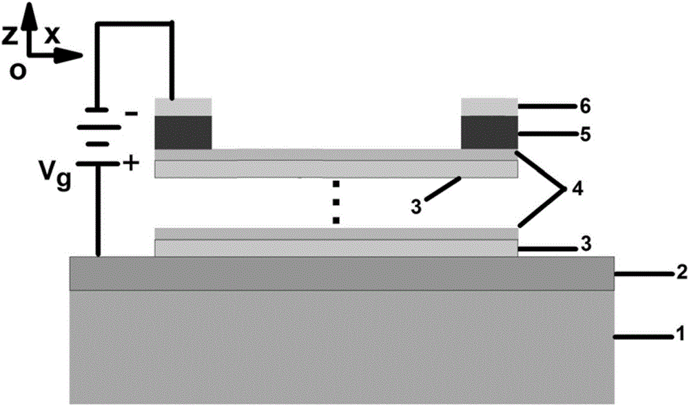
[0043] refer to figure 1 , the fabrication method of the terahertz wave graphene complementary microstructure modulator of the present invention is as follows:

[0044] Step 1, making a flexible substrate

[0045] A common Si sheet is used as the sacrificial layer 7, and the solution containing the plastic flexible substrate 1 is sprayed on it by spin coating, and then dried in an oven for about 30 minutes. The temperature range in the oven is 150-200 ℃, and then use a high temperature furnace in an inert gas (or N 2 ) in a protective atmosphere to 300-400 ° C to form a uniform thin layer of flexible substrate.

[0046] In order to reduce the influence of the flexible substrate, its thickness is controlled at about 1-10 μm, preferably less than 5 μm.

[0047] Step 2, making an epitaxial layer doped with Si

[0048] A doped Si layer 2 with a thickness of 1-10 μm is formed by an epitaxial growth method, and the doping concentration is 2×10 16 cm -3, The electrical conducti...


PUM

PropertyMeasurementUnit
Layer thicknessaaaaaaaaaa
Thicknessaaaaaaaaaa
Thicknessaaaaaaaaaa

Abstract

The invention provides a terahertz modulator with a graphene complementary microstructure as an active area. The modulator comprises a substrate, a doped semiconductor layer growing on the substrate, an insulating layer and an active area layer which are sequentially stacked, and an electrode growing on the topmost active area layer, wherein the insulating layer at the bottommost grows on the doped semiconductor layer, the active area layer is arranged on the top, and the active area layer is a graphene layer with the complementary microstructure. The invention further provides a manufacturing method of the terahertz modulator. The Fermi level of graphene is changed through external bias, and accordingly deep modulation of incident THz waves is achieved.

Description

technical field [0001] The invention relates to a terahertz graphene microstructure modulator, in particular to a design for effectively modulating terahertz waves by using graphene complementary microstructures. Background technique [0002] Terahertz (terahertz, THz, 1THz = 10 12 Hz=4.1meV) wave is between microwave and infrared radiation in the electromagnetic spectrum, and its frequency ranges from 0.3THz to 10THz. It is in the transition region from electronics to photonics, and has great application value in national economy and national security. The energy of terahertz wave photons matches the energy of low-frequency vibration and rotation of material material molecules. It is significantly different from microwave and infrared light in terms of propagation, reflection and absorption. It is used in short-range wireless communication, object imaging, biological detection and It has great application prospects in astronomical observation. However, due to the lack of ...

Claims


Application Information

Patent Timeline
IPC IPC(8): G02F1/015
CPCG02F1/015G02F2203/13
Inventor 何晓勇刘峰林方婷石旺舟
Owner SHANGHAI NORMAL UNIVERSITY
Why Eureka
Try Eureka