Touch substrate, manufacturing method thereof, and touch screen
A manufacturing method and touch screen technology, applied in programmable/customizable/modifiable circuits, instruments, circuit electrostatic discharge protection, etc., can solve the problems of insulation performance degradation, black matrix pattern resistivity reduction, etc., to avoid ESD , Improve the effect of anti-ESD ability
- Summary
- Abstract
- Description
- Claims
- Application Information
AI Technical Summary
Problems solved by technology
Method used
Image
Examples
Embodiment 1
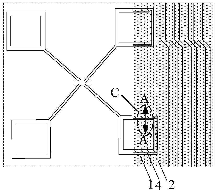
[0036] This embodiment provides a touch substrate, including a touch area on the base substrate 3 and a wiring area around the touch area, such as image 3 As shown, the wiring area includes: a black matrix pattern 2 covering the wiring area; a conductive wiring 1 located on the black matrix pattern 2, wherein two adjacent conductive wirings 1 located on the black matrix pattern 2 are arranged Conductive pattern 4 with ground.
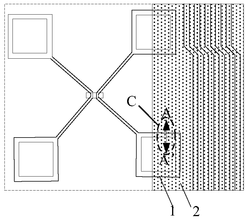
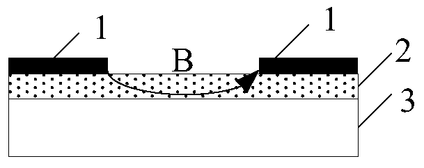
[0037] On the black matrix pattern, due to the decrease of the resistivity of the black matrix pattern, the ESD phenomenon is prone to occur between two adjacent conductive traces, so in this embodiment, the adjacent two conductive traces on the black matrix pattern There is a grounded conductive pattern between them, which can conduct away the static electricity between two adjacent conductive traces, thereby avoiding ESD between two adjacent conductive traces, thereby improving the ESD resistance of the touch substrate ability.
[0038] Preferably,...
Embodiment 2
[0044] like Figure 5 As shown, the present embodiment provides a touch screen, which includes the above-mentioned touch substrate, and further includes a protective structure 5 covering the touch substrate. The touch screen of this embodiment can be applied to human-computer interaction devices.
[0045] Further, the touch screen also includes a grounding point located outside the touch substrate, such as Figure 5 As shown, the protective structure 5 is provided with a via hole, and the conductive pattern 4 is electrically connected to a ground point outside the touch substrate through the via hole, so that the conductive pattern 4 can be grounded through the ground point.
[0046] Further, as Figure 5 As shown, the touch screen also includes:
[0047] The conductive lead 6 that runs through the via hole and connects the conductive pattern and the ground point, and the static electricity between adjacent conductive traces 1 is transferred to the ground point through the ...
Embodiment 3
[0050] This embodiment provides a method for manufacturing a touch substrate. The touch substrate includes a touch area and a wiring area surrounding the touch area. The manufacturing method includes forming a black matrix pattern in the wiring area and forming a black matrix pattern on the black matrix pattern. Conductive traces, such as Figure 4 As shown, the preparation method also includes:
[0051] A grounded conductive pattern 4 is formed between two adjacent conductive traces 1 .
[0052] On the black matrix pattern, due to the decrease of the resistivity of the black matrix pattern, the ESD phenomenon is prone to occur between two adjacent conductive traces, so in this embodiment, the adjacent two conductive traces on the black matrix pattern There is a grounded conductive pattern between them, which can conduct away the static electricity between two adjacent conductive traces, thereby avoiding ESD between two adjacent conductive traces, thereby improving the ESD re...
PUM
 Abstract
Description
Claims
Application Information


