Touch panel and making method thereof and touch device

A touch panel, non-touch technology, applied in instruments, electrical digital data processing, data processing input/output process, etc., can solve the problems affecting product yield, weak anti-static ability, and high impedance of metal bridge wires. Achieve the effect of reducing electrostatic breakdown, preventing electrostatic breakdown connecting bridges, and improving yield

Inactive Publication Date: 2016-12-07
BOE TECH GRP CO LTD +1
View PDF8 Cites 13 Cited by
  • Summary
  • Abstract
  • Description
  • Claims
  • Application Information

AI Technical Summary

Problems solved by technology

[0004] The wiring of the capacitive touch panel includes a plurality of sensing electrode layers arranged in parallel at intervals, a plurality of driving electrode layers separated by the sensing electrode layers, and two conductive electrode layers arranged in para

Method used


Image

  • Touch panel and making method thereof and touch device
  • Touch panel and making method thereof and touch device
  • Touch panel and making method thereof and touch device

Examples


Embodiment 1

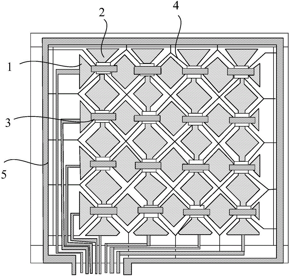
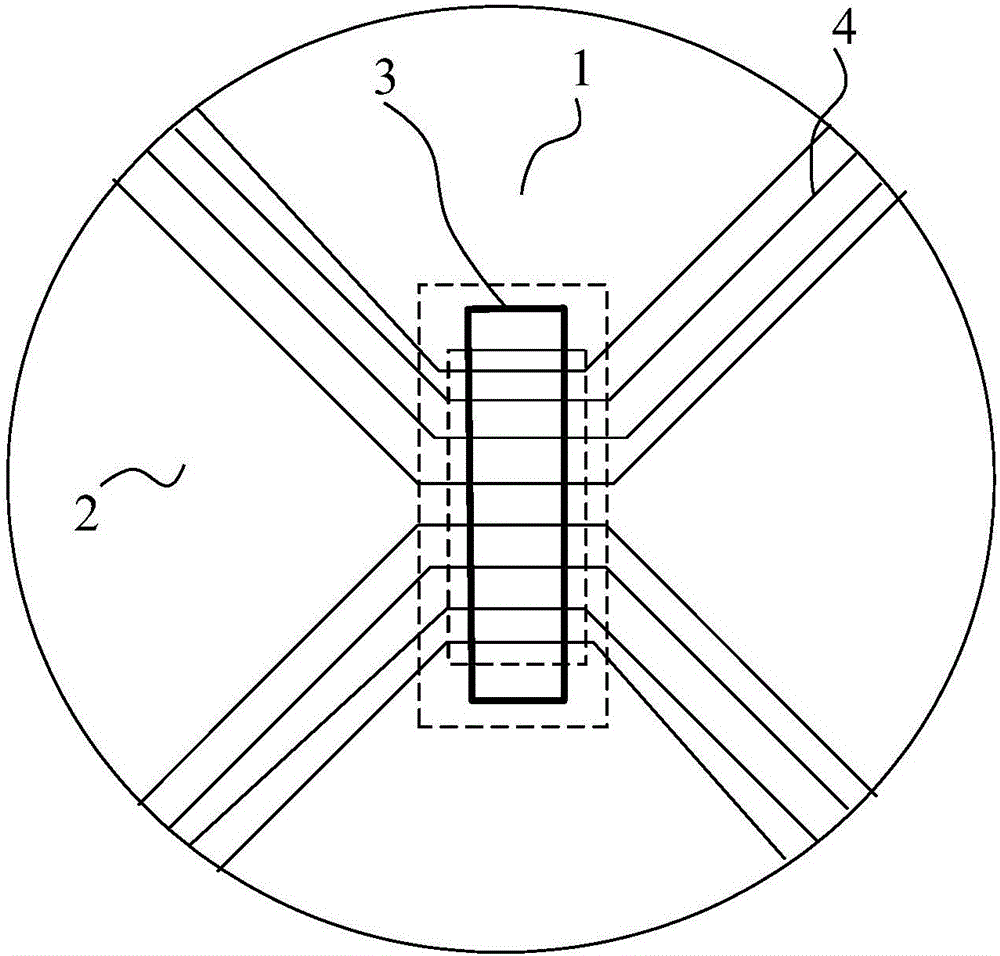
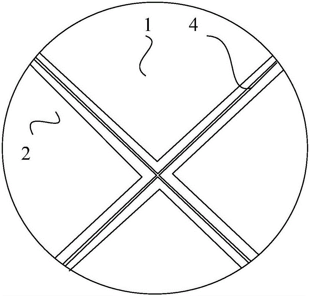
[0032] Such as figure 1 as shown, figure 1 Schematic diagram of the structure of the touch panel provided by the embodiment of the present invention; the present invention provides a touch panel, including: the first electrode and the second electrode located on the same layer and intersecting each other in the touch area, located in the non-touch area The ground wiring in the control area, wherein: the first electrode includes a plurality of first sub-electrode blocks 1 arranged along the first direction, the second electrode includes a plurality of second sub-electrode blocks 2 arranged along the second direction, and along In the second direction, any two adjacent second sub-electrode blocks 2 are connected to each other, along the first direction, any adjacent two first sub-electrode blocks 1 are bridged by a connecting bridge 3, the first direction and The second direction is vertical; also includes:

[0033] At least one set of electrostatic lead-out lines 4 that are i...

Embodiment 2

[0045] The present invention also provides a touch device, comprising: the touch panel described in any one of the above. Since the above-mentioned touch panel can reduce the phenomenon of electrostatic breakdown, the touch device provided by the present invention has a better yield rate.

Embodiment 3

[0047] Such as Figure 5 as shown, Figure 5 It is a flowchart of a method for manufacturing a touch panel provided by an embodiment of the present invention. The present invention also provides a method for manufacturing a touch panel, including:

[0048] Step S501: forming first electrodes and second electrodes on the same layer in the touch area and intersecting each other on the base substrate, and ground traces located in the non-touch area, wherein: the first electrode includes a plurality of edges The first sub-electrode blocks arranged in the first direction, the second electrode includes a plurality of second sub-electrode blocks arranged in the second direction, and along the second direction, any two adjacent second sub-electrode blocks are connected to each other , along the first direction, any two adjacent first sub-electrode blocks are bridged by a connecting bridge, and the first direction is perpendicular to the second direction; it also includes:

[0049] Ste...


PUM


Abstract

The invention discloses a touch panel and a making method thereof and a touch device, and the touch panel and the touch device are used for reducing the electrostatic breakdown phenomenon. The touch panel comprises a first electrode, a second electrode, a grounding line located in a non-touch area and at least one group of mutually insulated electrostatic guide lines which are arranged between the first electrode and the second electrode; the first electrode and the second electrode are located on the same layer in a touch area and arranged in a mutually crossed mode; the first electrode comprises multiple first sub electrode blocks which are arranged in the first direction, the second electrode comprises multiple second sub electrode blocks which are arranged in the second direction, every two adjacent second sub electrode blocks are connected with each other in the second direction, every two adjacent first sub electrode blocks are connected in a bridged mode through a connection bridge in the first direction, and the first direction is perpendicular to the second direction; each group of the electrostatic guide lines walk along gaps between every two adjacent first sub electrode block and second electrode block in the touch area and pass through at least one bridge connection area and are conductive with the grounding line in the non-touch area.

Description

technical field [0001] The invention relates to the field of touch technology, in particular to a touch panel, a manufacturing method thereof, and a touch device. Background technique [0002] A liquid crystal display is a commonly used flat panel display at present, and a thin film transistor liquid crystal display (Thin Film Transistor Liquid Crystal Display, TFT-LCD for short) is a mainstream product in the liquid crystal display. [0003] Electrostatic breakdown is a very common damage mode in the electronics industry. It is a phenomenon caused by electrostatic discharge of a large amount of static electricity concentrated to a certain part of the device. Electrostatic breakdown will cause very serious damage to TFT-LCD devices, and it needs to be avoided as much as possible during the manufacturing process of TFT-LCD devices. [0004] The wiring of the capacitive touch panel includes a plurality of sensing electrode layers arranged in parallel at intervals, a plurality...

Claims


Application Information

Patent Timeline
IPC IPC(8): G06F3/044
CPCG06F3/044G06F2203/04103G06F2203/04111
Inventor 李君胡明张雷郭总杰刘祖文
Owner BOE TECH GRP CO LTD
Why Eureka
Try Eureka