
Ion implantation equipment and monitoring method

A technology of ion implantation equipment and electronic counter, which is applied to discharge tubes, electrical components, circuits, etc., and can solve problems such as unstable annealing process, unstable measuring machine, and differences in semiconductor substrates themselves.

Active Publication Date: 2018-08-24
SHANGHAI HUALI MICROELECTRONICS CORP
View PDF6 Cites 0 Cited by
  • Summary
  • Abstract
  • Description
  • Claims
  • Application Information

AI Technical Summary

Problems solved by technology

[0006] The problem to be solved by the present invention is to propose an ion implantation equipment and monitoring method, which solves the external interference caused by the difference of the semiconductor substrate itself, the unstable annealing process, and the instability of the measuring machine when the semiconductor substrate is used to monitor the high-energy ion implantation. , and the method of the present invention can measure and monitor the dose of actual dopant ions in the semiconductor substrate

Method used


Image

  • Ion implantation equipment and monitoring method
  • Ion implantation equipment and monitoring method

Examples


Embodiment Construction

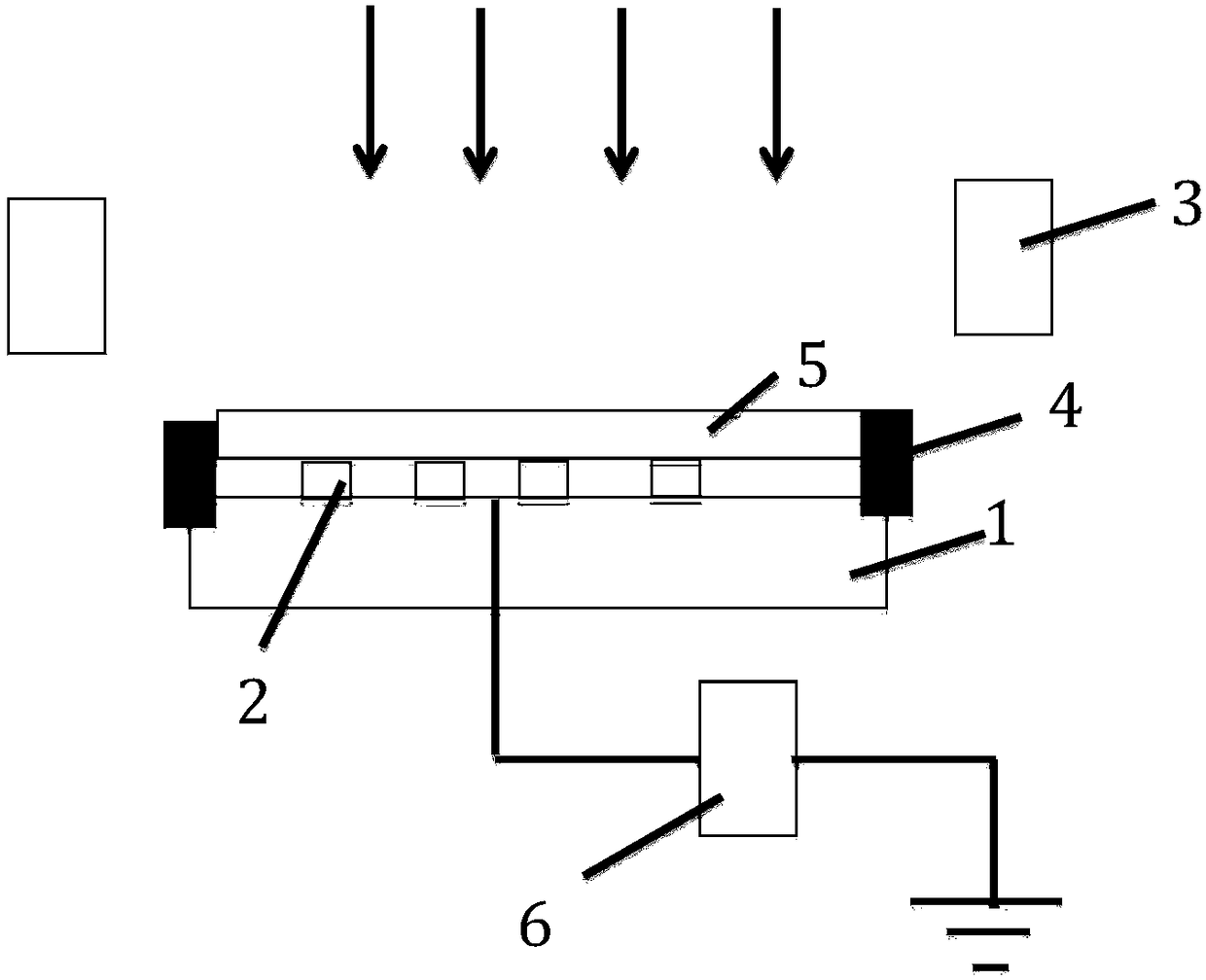
[0025] The existing technology monitors the dose of ion implantation equipment on the semiconductor substrate, and anneals the semiconductor substrate and measures the sheet resistance to monitor the dose of doping ions in the semiconductor substrate, assisting the dose monitoring system of the ion implantation equipment monitor. However, the use of monitoring semiconductor substrate monitoring is vulnerable to external interference, such as the differences in the semiconductor substrate itself, unstable annealing process, unstable measuring machine and other external interference.

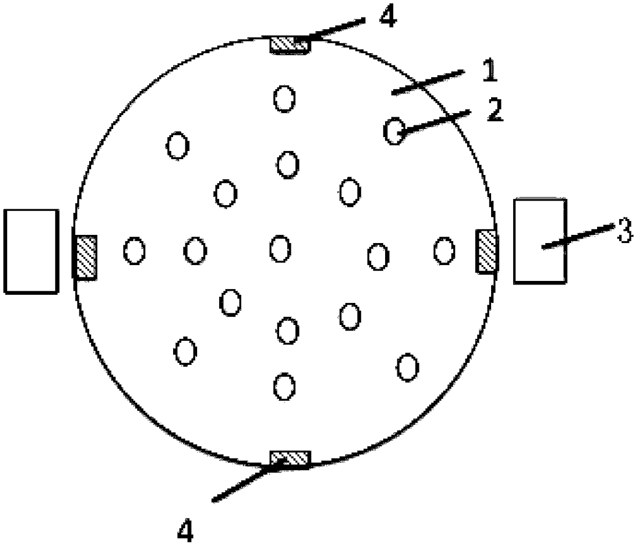
[0026] In order to solve the above-mentioned problems, the present invention provides an ion implantation device, comprising: a process chamber and a carrying platform located in the process chamber, the carrying platform is used for placing and monitoring a semiconductor substrate, and also includes:

[0027] The electromagnetic field providing unit is arranged on both sides of the carrying platf...


PUM


Abstract

The invention provides ion implantation equipment and a monitoring method therefor. The ion implantation equipment comprises a process cavity and a bearing platform positioned in the process cavity, wherein the bearing platform is used for placing a monitoring semiconductor substrate; the ion implantation equipment also comprises electromagnetic field supplying units, grounding units and an electronic counter, wherein the electromagnetic field supplying units are arranged on the two sides of the bearing platform and used for forming an electromagnetic field on the two sides of the bearing platform; the electromagnetic field is used for filtering secondary electrons during monitoring the ion implantation equipment; the grounding units are used for enabling the monitoring semiconductor substrate to be grounded during monitoring the ion implantation equipment; and the electronic counter is electrically connected with the grounding units and used for calculating the dosage of the doped ions in the monitoring semiconductor substrate during monitoring the ion implantation equipment. By adoption of the ion implantation equipment and the monitoring method therefor, the problems existing in high-energy ion implantation monitoring through the monitoring semiconductor substrate caused by difference of the semiconductor substrate, an instable annealing process, an instable measurement machine table and other external interferences are solved; and in addition, the dosage of the actually doped ions in the semiconductor substrate can be detected.

Description

technical field [0001] The invention relates to the technical field of semiconductors, in particular to an ion implantation device and a monitoring method. Background technique [0002] With the continuous evolution of semiconductor technology nodes, the requirements for the doping ion dose accuracy of ion implantation process are getting higher and higher, and the dose resolution and absolute dose accuracy need to reach a very high level. The current mainstream control method for ion implantation equipment is to use a closed-loop Faraday system located on both sides or behind the mounting table that fixes the semiconductor substrate, and control the implantation dose of the ion beam through the charge integrator in the closed-loop Faraday system. Although the nominal dose in the charge integrator is proportional to the dose of dopant ions implanted into the semiconductor substrate, due to factors such as reflection on the semiconductor substrate, ion loss by sputtering, and...

Claims


Application Information

Patent Timeline
Patent Type & Authority Patents(China)
IPC IPC(8): H01J37/317H01J37/244
CPCH01J37/244H01J37/3171
Inventor 邱裕明肖天金
Owner SHANGHAI HUALI MICROELECTRONICS CORP
Learn More