Lead width and lead space detection method and device for lead in PCB image

An image-in-line-width technology, applied in measurement devices, image enhancement, image analysis, etc., can solve the problem of cumbersome detection process, and achieve the effect of simple and fast detection process

Inactive Publication Date: 2016-12-14
BEIJING LUSTER LIGHTTECH
View PDF4 Cites 9 Cited by
  • Summary
  • Abstract
  • Description
  • Claims
  • Application Information

AI Technical Summary

Problems solved by technology

[0007] The purpose of the embodiments of the present invention is to provide a method and device for detecting the line width and line spacing of the conductors in the PCB imag

Method used


Image

  • Lead width and lead space detection method and device for lead in PCB image
  • Lead width and lead space detection method and device for lead in PCB image
  • Lead width and lead space detection method and device for lead in PCB image

Examples


Example Embodiment

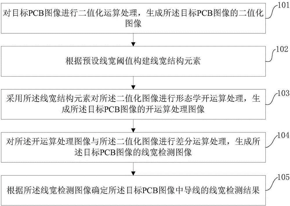
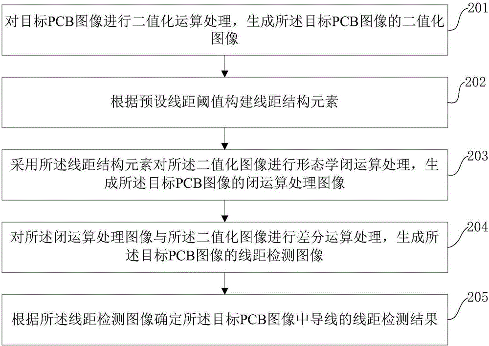
[0076] In order to enable those skilled in the art to better understand the technical solutions in the present invention, the following will clearly and completely describe the technical solutions in the embodiments of the present invention with reference to the accompanying drawings in the embodiments of the present invention. Obviously, the described The embodiments are only a part of the embodiments of the present invention, rather than all the embodiments. Based on the embodiments of the present invention, all other embodiments obtained by those of ordinary skill in the art without creative work shall fall within the protection scope of the present invention.

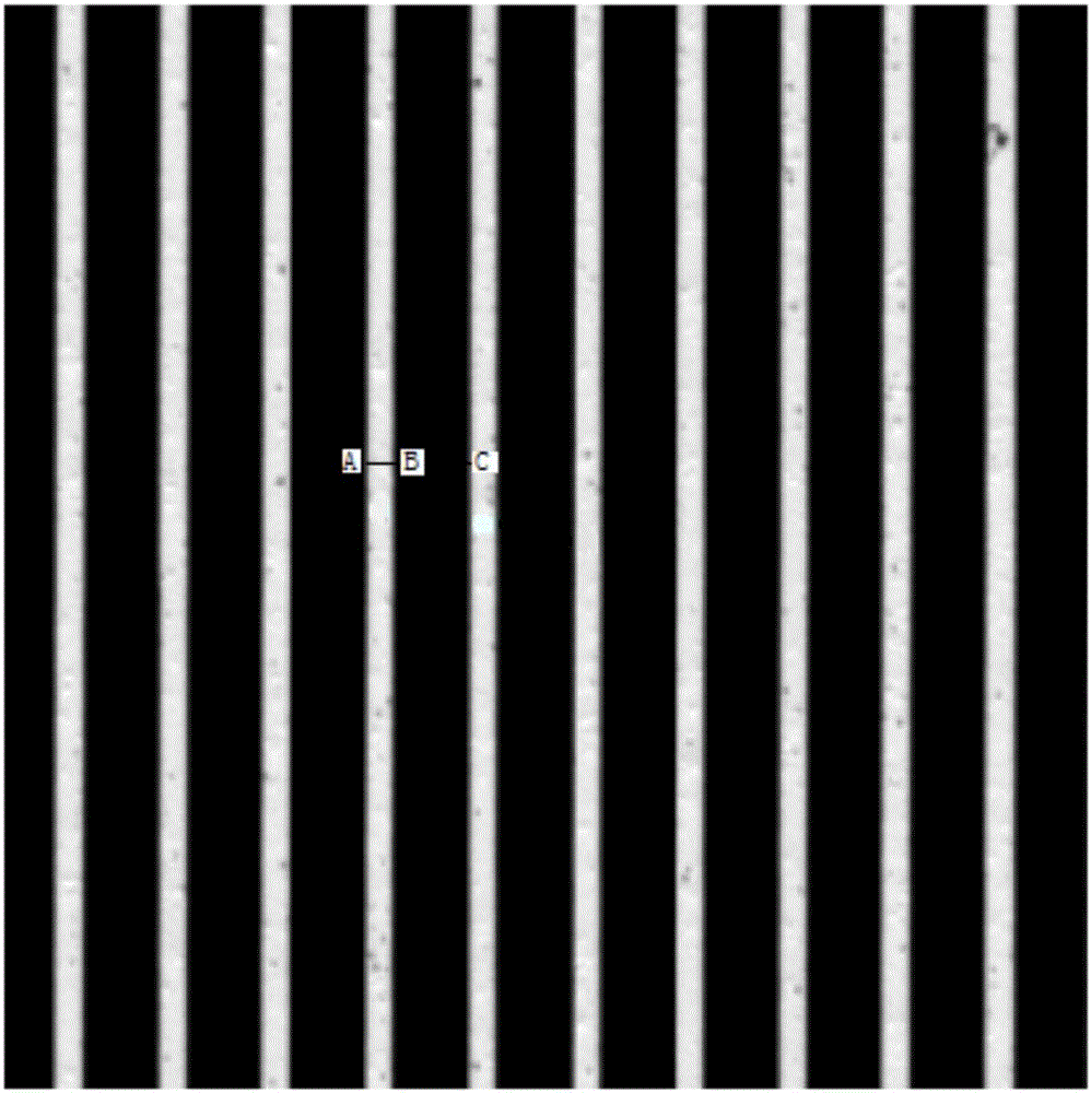
[0077] The present invention provides a method and device for detecting the line width and line distance of wires in a PCB image. Through the method provided by the embodiment of the present invention, as long as the binary image of the target PCB image is respectively subjected to morphological opening operations or T...


PUM


Abstract

The invention discloses a lead width and lead space detection method and device for a lead in a PCB image. The lead width detection method comprises the steps that binary operation processing is performed on a target PCB image so that the binary image of the target PCB image is generated; lead width structural elements are constructed according to a preset lead width threshold; morphological opening operation processing is performed on the binary image by using the lead width structural elements so that the opening operation processing image of the target PCB image is generated; difference operation processing is performed on the opening operation processing image and the binary image so that the lead width detection image of the target PCB image is generated; and the lead width detection result of the lead in the target PCB image is determined according to the lead width detection image. The lead width and the lead space of the lead in the PCB image are detected by the method so that the detection process is simpler and more rapid.

Description

Technical field [0001] The invention relates to the technical field of PCB board detection, in particular to a method and device for detecting the line width and line distance of wires in a PCB image. Background technique [0002] Generally, there are various lines on the designed PCB board. When arranging each line, there are certain requirements for the line width and line spacing of the wires in the line. The line width is For a wire, any straight line along the normal direction of the wire that intersects the boundary on the opposite sides of the wire will produce two intersection points. The distance between these two intersection points is defined as the line width of the wire (for example figure 1 The distance between the two points A and B); the line distance is for two or more wires, for two adjacent wires, any straight line along the normal direction of the wire is adjacent to the two wires After the two boundaries of the intersecting, two intersections will be generate...

Claims


Application Information

Patent Timeline
IPC IPC(8): G06T7/00G01B11/04G01B11/14
CPCG06T7/0004G01B11/046G01B11/14G06T2207/10004G06T2207/30141
Inventor 杨艺孟凡清金刚姚毅
Owner BEIJING LUSTER LIGHTTECH
Why Eureka
Try Eureka