Printing mechanism for manufacturing semiconductor modules and working method thereof

A printing mechanism and semiconductor technology, which is applied in semiconductor/solid-state device manufacturing, typewriters, printing devices, etc., can solve problems such as the inability to guarantee long-term efficient and stable operation of printing work, the complicated operation process of printing mechanisms, and real-time monitoring of inoperable status. Achieve the effect of low operating cost, smooth and efficient operation process, and improved printing efficiency

Inactive Publication Date: 2017-01-04
TAICANG GAOCHUANG ELECTRICAL TECH
View PDF11 Cites 2 Cited by
  • Summary
  • Abstract
  • Description
  • Claims
  • Application Information

AI Technical Summary

Problems solved by technology

[0004] 1. The overall structure and operation process of the printing mechanism are very complicated, and the load requirements are high, the maintenance is very cumbersome, and the manufacturing and operating costs are high;
[0005] 2. The degree of automation is low, the operation of personnel is complicated, and the printing efficiency is

Method used


Image

  • Printing mechanism for manufacturing semiconductor modules and working method thereof

Examples


Embodiment 1

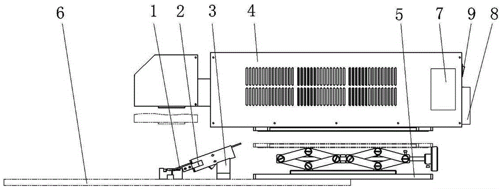
[0027] Such as figure 1 As shown, a printing mechanism for manufacturing semiconductor modules in this embodiment includes: a printing jaw 1, a jaw cylinder 2, a jaw cylinder seat 3, a laser printer 4, a printer bottom plate 5, a frame panel 6, a detection Device 7 , display panel 8 and emergency shutdown button 9 .

[0028] The connection relationship of the above-mentioned components is as follows: the jaw cylinder 2 is fixed on the frame panel 6 through the jaw cylinder base 3, a pair of printing jaws 1 are installed at the front end of the jaw cylinder 2, and the laser printer 4 passes through the printer. The bottom plate 5 is fixed on the frame panel 6; the surface of the laser printer 4 is respectively provided with a detection device 7, a display panel 8 and an emergency shutdown button 9, and the detection device 7 is connected to the display panel 8; the detection device 7 includes temperature sensor, humidity sensor and smoke sensor. Wherein the top of the detecti...


PUM


Abstract

The invention discloses a printing mechanism for manufacturing semiconductor modules and mainly relates to the technical field of semiconductor manufacturing. A clamping jaw air cylinder is fixed to a machine rack panel through a clamping jaw air cylinder seat; a pair of letter printing clamping jaws is arranged at the front end of the clamping jaw air cylinder; a laser printer is fixed to the machine rack panel through a printer bottom board; a detecting device, a display panel and an emergency shut-down button are arranged on the surface of the laser printer; the detecting device is connected with the display panel; and the detecting device comprises a temperature sensor, a humidity sensor and a smoke sensor. The whole structure of the printing mechanism and the operation process of the printing mechanism are very simple, maintenance is fast and convenient, cost is low, printing efficiency is high, the operation state of the printing mechanism can be conveniently monitored by operators, and long-term, efficient and stable operation can be ensured. The invention further discloses a working method of the printing mechanism for manufacturing the semiconductor modules.

Description

technical field [0001] The invention relates to the technical field of semiconductor manufacturing, in particular to a printing mechanism for manufacturing semiconductor modules and a working method of the printing mechanism. Background technique [0002] The semiconductor module is a device that produces stimulated emission by using a certain semiconductor material as a working substance, and is a part of the semiconductor laser. [0003] In recent years, with the continuous development of science and technology, related industries have higher and higher technical requirements for semiconductor modules. However, the existing printing mechanism for manufacturing semiconductor modules still has the following defects: [0004] 1. The overall structure and operation process of the printing mechanism are very complicated, and the load requirements are high, the maintenance is very cumbersome, and the manufacturing and operating costs are high; [0005] 2. The degree of automa...

Claims


Application Information

Patent Timeline
IPC IPC(8): B41J2/435B41J3/407B41J29/393B41J29/46H01L21/67
CPCB41J2/435B41J3/4073B41J29/393B41J29/46H01L21/67282
Inventor 程嘉义
Owner TAICANG GAOCHUANG ELECTRICAL TECH
Why Eureka
Try Eureka