Method of extracting contour and corner information in PCB design chart

A technology of PCB board and extraction method, which is applied in calculation, image enhancement, image analysis, etc., can solve the problems of poor extraction accuracy and achieve the effect of improving efficiency

Active Publication Date: 2017-01-04
合肥九川智能装备有限公司
View PDF4 Cites 7 Cited by
  • Summary
  • Abstract
  • Description
  • Claims
  • Application Information

AI Technical Summary

Problems solved by technology

[0005] An embodiment of the present invention provides a method for extracting outline and corner poin...

Method used


Image

  • Method of extracting contour and corner information in PCB design chart
  • Method of extracting contour and corner information in PCB design chart
  • Method of extracting contour and corner information in PCB design chart

Examples


Embodiment Construction

[0030] In order to enable those skilled in the art to better understand the technical solutions in the present invention, the technical solutions in the embodiments of the present invention will be clearly and completely described below in conjunction with the drawings in the embodiments of the present invention. Obviously, the described The embodiments are only some of the embodiments of the present invention, not all of them. Based on the embodiments of the present invention, all other embodiments obtained by persons of ordinary skill in the art without making creative efforts shall fall within the protection scope of the present invention.

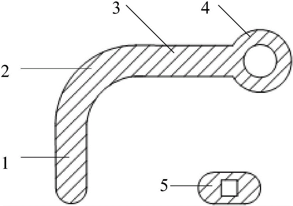
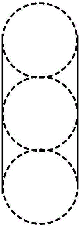
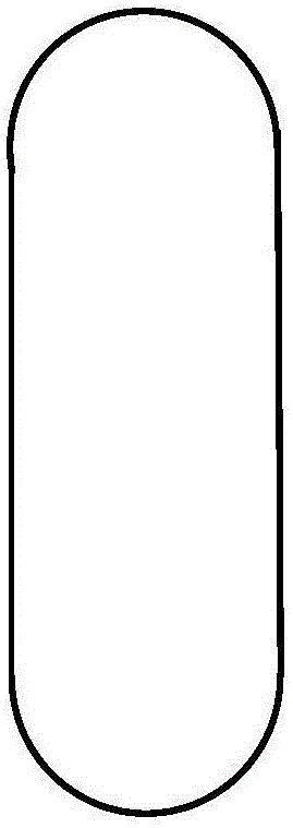
[0031] The CAM data of PCB design drawings generally include the following types of drawing items, including straight lines, arcs, composite polygons, standard circular pads, and standard rectangular pads (standard circular pads are closed circles, and the interior may Contains a small round or square hole), standard round rectangular p...


PUM


Abstract

The invention discloses a method of extracting contour and corner information in a PCB design chart. The method comprises steps: CAM data of the PCB design chart are analyzed, all drawing items and a drawing sequence are determined, and according to the drawing sequence, coordinate information of each drawing item in the PCB design chart is extracted sequentially; according to a trajectory formed by moving of the coordinate information, a vector aperture is used for converting each drawing item to a closed vector graph; the graph polarity information of the closed vector graph is judged, closed vector graphs with a connected conversion sequence and the same graph polarity are divided into one group, intra-group operation is firstly carried out, between-group operation is then carried out, and the contour and corner information in the PCB design chart can be obtained. the accuracy of vector data of each drawing item is not lost during the equivalent conversion process from the vector data to the vector graph, an algorithm for a graph Boolean operation is improved, and the operation efficiency is improved. The contour and corner information obtained by the extraction method of the invention is more accurate.

Description

technical field [0001] The invention relates to the technical field of PCB board detection, in particular to a method for extracting outline and corner point information in a PCB board design drawing. Background technique [0002] Due to process reasons, there may be macroscopic defects such as open circuits, short circuits, burrs, gaps, pinholes, and copper slag on the actual PCB board (Printed Circuit Board, printed circuit board). Only by identifying these defects can we provide a basis for repairing the defects. The process of defect determination is (1) establishing a detection reference model, which is a model that records the outline and corner point information of the circuit on the PCB board in the design drawing, and the corner point refers to the boundary point between the circuit outline segments; (2) Utilize the image collector to collect the image information of the actual circuit outline and corner points on the PCB produced according to the above-mentioned d...

Claims


Application Information

Patent Timeline
IPC IPC(8): G06T7/00
CPCG06T7/0004G06T2207/20164G06T2207/30141
Inventor 杨艺吴秀永金刚赵严
Owner 合肥九川智能装备有限公司
Why Eureka
Try Eureka