Welding structure and welding method for PCB and FPCB
A welding method and pad technology, applied in metallurgical bonding, electrical components, printed circuit manufacturing, etc., can solve the problems of poor circuit board welding effect and complicated welding process, and achieve simple and easy operation and alignment. Simple, efficient results
- Summary
- Abstract
- Description
- Claims
- Application Information
AI Technical Summary
Problems solved by technology
Method used
Image
Examples
Embodiment Construction
[0051] The following will clearly and completely describe the technical solutions in the embodiments of the present invention with reference to the accompanying drawings in the embodiments of the present invention. Obviously, the described embodiments are only some, not all, embodiments of the present invention. Based on the embodiments of the present invention, all other embodiments obtained by persons of ordinary skill in the art without creative efforts fall within the protection scope of the present invention.
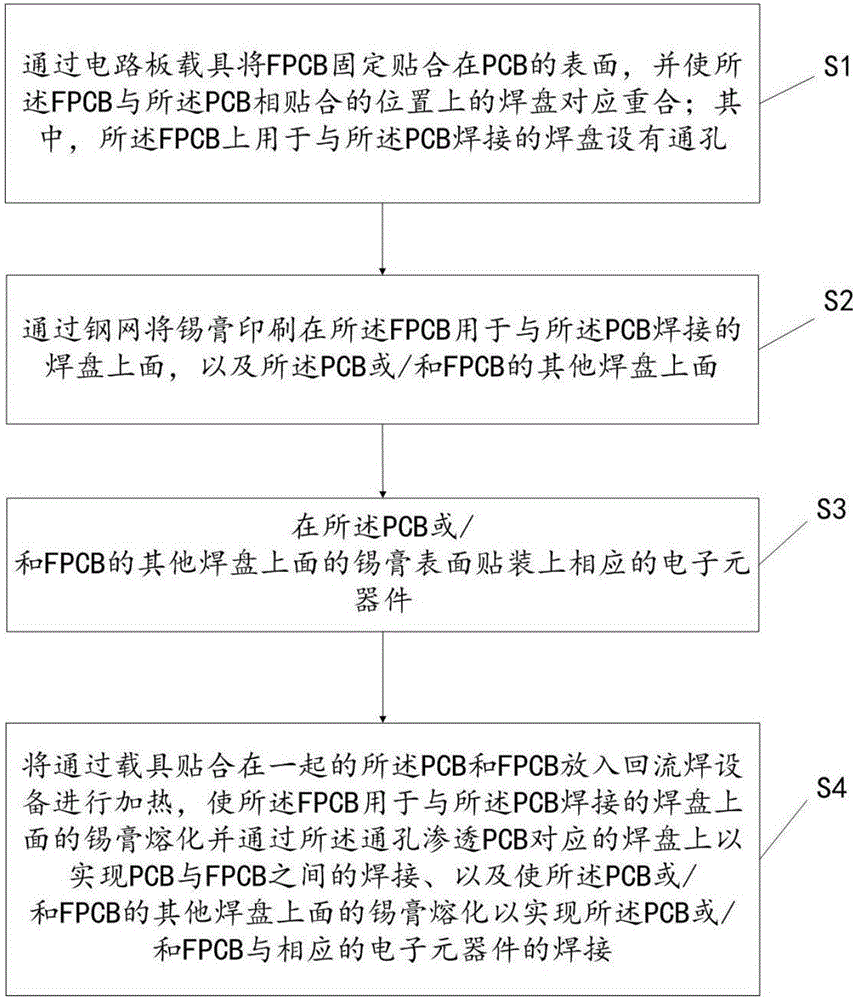
[0052] A preferred embodiment of the present invention provides a method for realizing welding between a PCB and an FPCB. In this embodiment, the soldering pad on the FPCB to be welded is provided with a through hole for welding with the PCB. see figure 1 , figure 1 Realize the flowchart of the soldering method between PCB and FPCB for this embodiment, comprise the following steps:
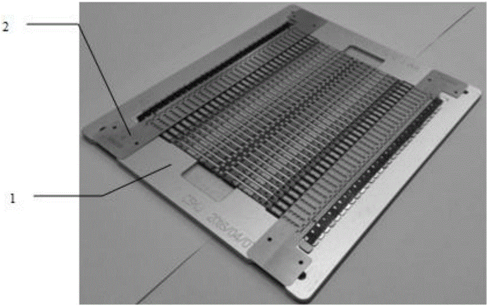
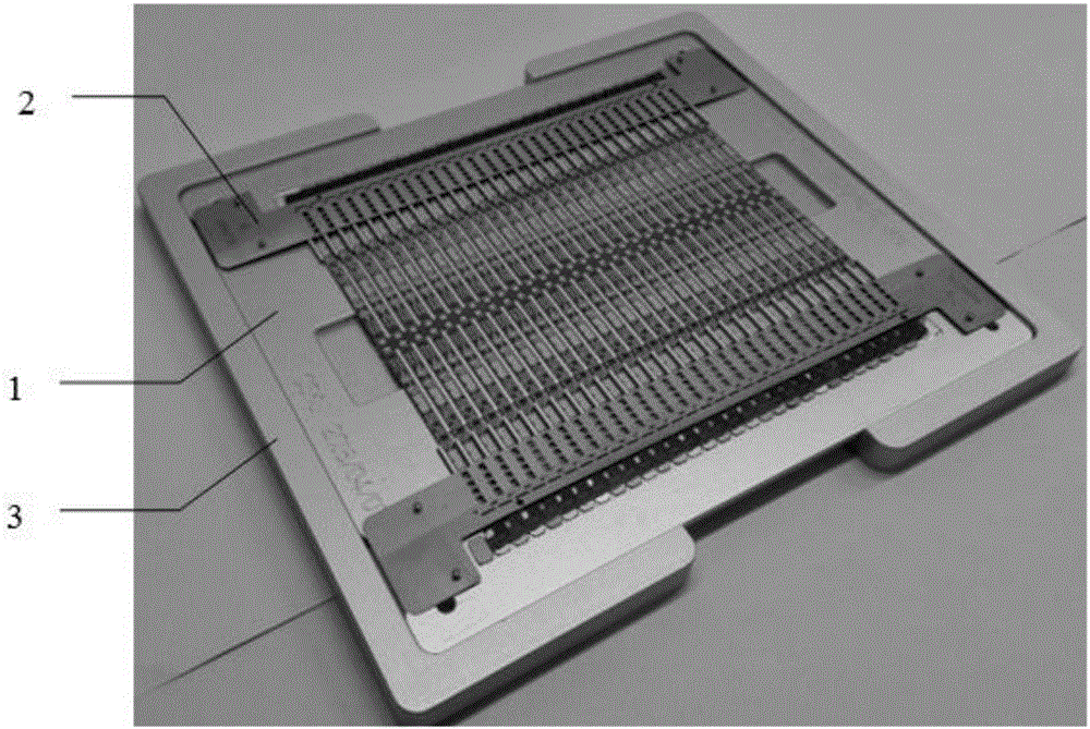
[0053] S1. Fix the FPCB on the surface of the PCB through the circuit board carr...
PUM
 Abstract
Description
Claims
Application Information


