Focusing shock wave excitation device for performing non-contact excitation on MEMS (micro electro mechanical system) micro structure

A non-contact, excitation device technology, applied in microstructure devices, microstructure technology and other directions, can solve the problems of difficult dynamic characteristic parameters of microstructures, and achieve the effects of easy dynamic characteristic parameters, avoiding interference, and facilitating testing.

Inactive Publication Date: 2017-01-11
BOHAI UNIV
View PDF7 Cites 2 Cited by
  • Summary
  • Abstract
  • Description
  • Claims
  • Application Information

AI Technical Summary

Problems solved by technology

However, the main disadvantage of this device is that the device uses an elastic base to excite the microstructure, so when the non-contact optical vibration measurement method is used to test the dynamic characteristics of the microstructure, the vibration response obtained The signal will inevitably contain the vibration response of the base structure, which will make it very difficult to obtain the dynamic characteristic parameters of the microstructure

Method used


Image

  • Focusing shock wave excitation device for performing non-contact excitation on MEMS (micro electro mechanical system) micro structure
  • Focusing shock wave excitation device for performing non-contact excitation on MEMS (micro electro mechanical system) micro structure
  • Focusing shock wave excitation device for performing non-contact excitation on MEMS (micro electro mechanical system) micro structure

Examples


Embodiment Construction

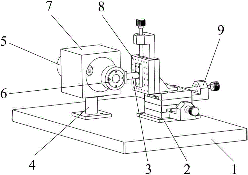
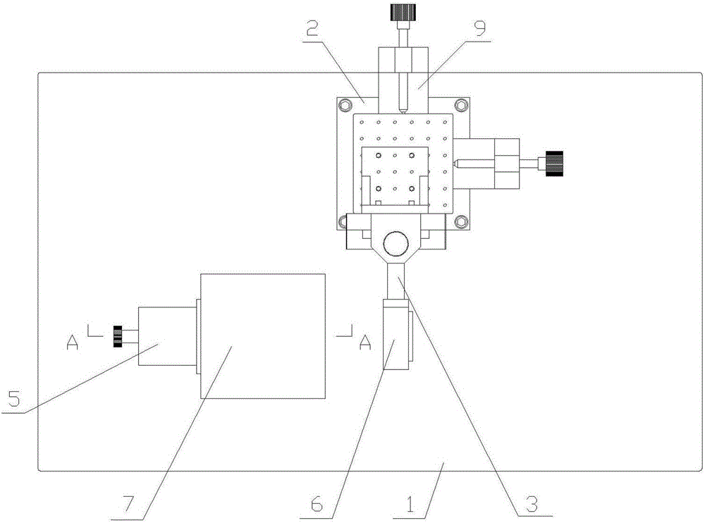
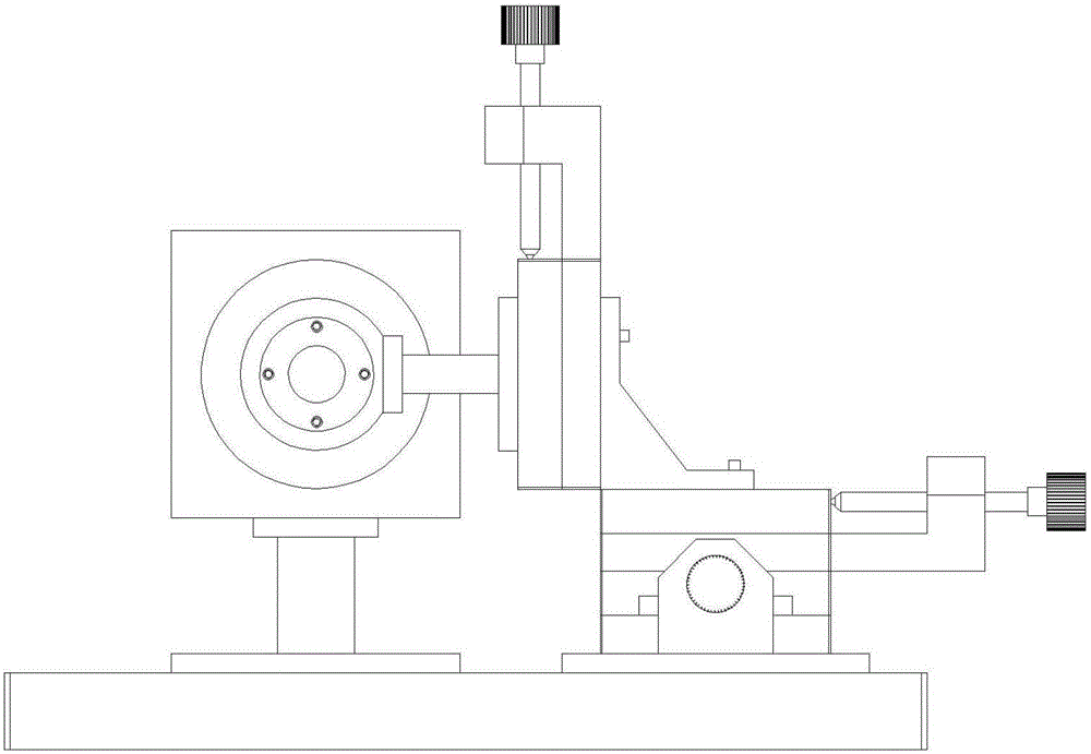
[0027] Such as Figure 1-Figure 8 As shown, the present invention relates to a focused shock wave excitation device for non-contact excitation of MEMS microstructures, including a substrate 1, on which a manual three-axis displacement table 9 and a support 4 are arranged, and the manual three-axis The axial displacement stage 9 is installed on a bottom plate 2, and the bottom plate 2 is fixed on the base plate 1 by screws. A microstructure unit 6 is provided on the Z-axis slide plate 8 of the manual three-axis displacement table 9; the microstructure unit 6 includes a mounting sleeve 601 installed on the Z-axis slide plate 8 through a horizontal support 3, and The mounting sleeve 601 is provided with a stepped mounting hole, and a MEMS microstructure 605 is installed at the bottom of the mounting hole through a microstructure mounting plate 607; the microstructure mounting plate 607 is fixed in the mounting hole by screws 606 uniformly distributed around the circumference On ...


PUM


Abstract

The invention discloses a focusing shock wave excitation device for performing non-contact excitation on an MEMS (micro electro mechanical system) micro structure. The focusing shock wave excitation device comprises a base plate, wherein a manual three-axis displacement table and a support seat are arranged on the base plate; a micro structure unit is arranged on a Z-axis slide plate of the manual three-axis displacement table; an ellipsoid cavity with an inner cavity being half of an ellipsoid surface is arranged at the upper end of the support seat; the first focus point of the ellipsoid surface is positioned in the ellipsoid cavity; the micro structure unit is positioned at one side of a second focus point of the ellipsoid surface; a pin electrode unit is arranged on the ellipsoid cavity; two pin electrodes are electrically connected with two electrodes of a high-voltage capacitor; a first air switch is arranged between the high-voltage capacitor and one pin electrode; the distance between the pin points of the second pin electrodes is smaller than the maximum air breakdown gap after the high-voltage capacitor is sufficiently charged; the high-voltage capacitor is electrically connected to positive and negative electrodes of a high-voltage power supply. The focusing shock wave excitation device has the beneficial effects that the interference of the vibration response of the base structure on the test result can be avoided; the non-contact excitation on the MEMS micro structure is realized; the excitation effect is good; the dynamic feature parameters of the micro structure are convenient to obtain.

Description

technical field [0001] The invention belongs to the technical field of micromechanical electronic systems, in particular to a focused shock wave excitation device for non-contact excitation of MEMS microstructures. Background technique [0002] Due to the advantages of low cost, small size and light weight, MEMS microdevices have broad application prospects in many fields such as automobile, aerospace, information communication, biochemistry, medical treatment, automatic control and national defense. For many MEMS devices, the micro-displacement and micro-deformation of their internal microstructures are the basis for the realization of device functions. Therefore, accurate testing of dynamic characteristic parameters such as the amplitude, natural frequency, and damping ratio of these microstructures has become the key to developing MEMS products. important content. [0003] In order to test the dynamic characteristic parameters of the microstructure, it is first necessary...

Claims


Application Information

Patent Timeline
Patent Type & Authority Applications(China)
IPC IPC(8): B81C99/00
CPCB81C99/0035
Inventor 佘东生杨一柳魏泽飞杨祯山赵辉
Owner BOHAI UNIV
Why Eureka
Try Eureka