Display panel and preparation method thereof

A technology of display panel and metal layer, applied in instruments, semiconductor devices, optics, etc., can solve the problems of uneven cell thickness, affecting the picture quality of liquid crystal display panel, etc.

Inactive Publication Date: 2017-01-11
BOE TECH GRP CO LTD +1
View PDF7 Cites 5 Cited by
  • Summary
  • Abstract
  • Description
  • Claims
  • Application Information

AI Technical Summary

Problems solved by technology

[0005] In the process of magnetron sputtering, the particles impacted by the surface of the metal target must have a particle distribution difference between the central area 102 of the metal target and the splicing area 103 of the metal target, which is manifested in the central area 102 of the metal target and the splicing area 103 of the metal target. The difference in metal film thickness causes the thickness of the metal thin film deposited on the glass substrate 20 to be periodically distributed, thereby causing the cell thickness of the liquid crystal display panel after the cell is also to be periodically changed, that is, the cell thickness is uneven (such as figure 2 shown)
Among them, the color temperature of the thicker box is relatively small and the color is warmer, and the color temperature of the thinner box is higher and the color is cooler, resulting in a periodic distribution of colors when displayed on the display panel, which seriously affects the picture of the LCD panel. quality

Method used


Image

  • Display panel and preparation method thereof
  • Display panel and preparation method thereof
  • Display panel and preparation method thereof

Examples


Embodiment Construction

[0037] The following will clearly and completely describe the technical solutions in the embodiments of the present invention with reference to the accompanying drawings in the embodiments of the present invention. Obviously, the described embodiments are only some, not all, embodiments of the present invention. Based on the embodiments of the present invention, all other embodiments obtained by persons of ordinary skill in the art without making creative efforts belong to the protection scope of the present invention.

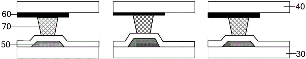
[0038] An embodiment of the present invention provides a display panel, such as image 3 As shown, it includes a first substrate 30 and a second substrate 40 set to the box; a metal layer 50, a black matrix 60 and a spacer 70 are arranged between the first substrate 30 and the second substrate 40; the spacer Object 70 , black matrix 60 and metal layer 50 , the orthographic projections of any two on the first substrate 30 overlap at least partially; The sum of...


PUM


Abstract

An embodiment of the invention provides a display panel and a preparation method thereof, relates to the technical field of display and guarantees a uniform cell gap of a liquid crystal display panel. The display panel comprises a first substrate and a second substrate which are arranged in a cell assembly manner, wherein a metal layer, a black matrix and spacers are arranged between the first substrate and the second substrate; orthographic projection of any two of the spacers, the black matrix and the metal layer on the first substrate at least overlaps partially; the thickness sum of any spacer, the metal layer and the black matrix is identical in a position corresponding to the spacer in the direction perpendicular to the first substrate. The invention is used for preparing the display panel.

Description

technical field [0001] The invention relates to the field of display technology, in particular to a display panel and a preparation method thereof. Background technique [0002] Liquid Crystal Display (LCD for short) has the advantages of low radiation, small size, and low energy consumption, and is widely used in electronic products such as tablet computers, televisions, and mobile phones. [0003] The liquid crystal display panel includes an array substrate and a cell substrate, and a liquid crystal layer between them. The array substrate includes a metal layer, which is generally formed into a metal film by magnetron sputtering (Sputter). That is, make the plasma (Plasma) formed by radio frequency or DC voltage contain high-energy charged ions, so that the charged ions hit the surface of the metal target, and the target particles are knocked out from the surface, thereby depositing on the surface of the substrate to form a metal film. [0004] Among them, such as figu...

Claims


Application Information

Patent Timeline
Patent Type & Authority Applications(China)
IPC IPC(8): G02F1/1335G02F1/1339G02F1/1333
CPCG02F1/1333G02F1/133512G02F1/1339G02F1/133514G02F1/13394G02F1/13396H01L27/1248H01L27/124H01L27/1259
Inventor 吴鹏蒋学兵高吉磊
Owner BOE TECH GRP CO LTD
Why Eureka
Try Eureka