Array Substrate

A technology of array substrates and arrays, applied in instruments, nonlinear optics, optics, etc., can solve the problems of increased brightness, poor display brightness uniformity, and reduced brightness, and achieve the effect of reducing differences and improving display brightness uniformity.

Active Publication Date: 2017-01-18
SHANGHAI AVIC OPTOELECTRONICS +1
View PDF5 Cites 3 Cited by
  • Summary
  • Abstract
  • Description
  • Claims
  • Application Information

AI Technical Summary

Problems solved by technology

On the other hand, when along the Figure 1A When aligning the alignment direction in the color filter unit, because there is an angle between the boundary of the color filter unit and the alignment direction, and when aligning from the black matrix to the inside of the color filter unit along the D1 direction through the boundary of the color filter unit, due to the color filter The height difference between the boundary of the light unit and the interior of the color filter unit weakens the frictional alignment effect, resulting in a decrease in brightness; on the contrary, when aligning from the inside of the color filter unit to the black matrix through the boundary of the color filter unit along the D1 direction , due to the height difference between the boundary of the color filter unit and the interior of the color filter unit, the frictional alignment effect is enhanced, resulting in an increase in brightness
[0009] In this way, due to the existence of height difference, when along the Figure 1A When aligning in the alignment direction shown in , since the color filter unit is higher on the right and lower on the left, the brightness difference on the right side of the pixel is greater than that on the left side, resulting in uniform display brightness when viewing angles are different. poor sex problem

Method used


Image

  • Array Substrate
  • Array Substrate
  • Array Substrate

Examples


Embodiment Construction

[0028] The application will be further described in detail below in conjunction with the accompanying drawings and embodiments. It should be understood that the specific embodiments described here are only used to explain related inventions, rather than to limit the invention. It should also be noted that, for ease of description, only parts related to the invention are shown in the drawings.

[0029] It should be noted that, in the case of no conflict, the embodiments in the present application and the features in the embodiments can be combined with each other. The present application will be described in detail below with reference to the accompanying drawings and embodiments.

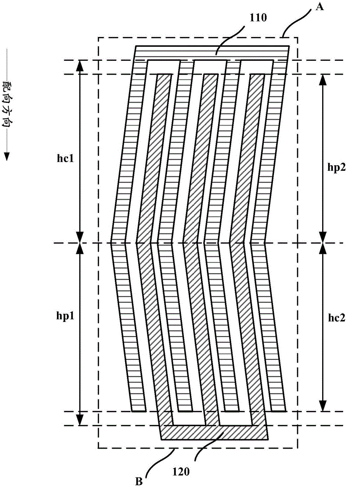
[0030] The array substrates in each embodiment of the present application include a plurality of scan lines extending along a first direction, a plurality of data lines extending along a second direction, and a plurality of display pixels formed by insulated intersections of the scan lines and data...


PUM


Abstract

This application discloses an array substrate, comprising: a plurality of scan line extending in the first direction; a plurality of data wire extending in the second direction; pixel arraywhich includes the multiple display pixels formed by crossing of scan line and data wire insulation; The array base plate also includes liquid crystal farmland array, which includes liquid crystal farmland groups of multiple array arrangements, and each liquid crystal farmland group includes the first liquid crystal farmland and the second liquid crystal farmland located along the second direction. A plurality of first electrode being parallel to each other is formed with the first liquid crystal farmland, and is formed with a plurality of second electrode being parallel to each other in the second liquid crystal farmland; First electrode and second electrode are different strip-shaped electric poles in different extending directions, and the lengthof the first electrode h1 and the length of the second electrode satisfies the condition: h1 =/ h2. This inverntion enhances the brightness uniformity of the display panel under different viewing angles.

Description

technical field [0001] The present disclosure generally relates to the field of display technology, and in particular, relates to an array substrate. Background technique [0002] Liquid crystal display panels are currently the mainstream technology in the display field. [0003] A liquid crystal display panel generally includes an array of display pixels. A pixel electrode and a common electrode are formed in each display pixel in the display pixel array. After applying different voltages to the pixel electrode and the common electrode, the liquid crystal molecules will deflect under the action of the electric field, thereby realizing the display of a predetermined picture. [0004] see Figure 1A Shown is a schematic structural diagram of a pixel electrode and a common electrode located in a display pixel in an existing liquid crystal display panel. Figure 1A In , the display pixel has a dual-domain structure. That is to say, in one display pixel, the shape of each str...

Claims


Application Information

Patent Timeline
Patent Type & Authority Applications(China)
IPC IPC(8): G02F1/1343G02F1/1362
CPCG02F1/134309G02F1/1362
Inventor 简守甫夏志强曹兆铿
Owner SHANGHAI AVIC OPTOELECTRONICS
Why Eureka
Try Eureka