Focused shock wave excitation device for dynamic feature testing of microstructure of MEMS (micro-electromechanical system)

A technology of excitation device and dynamic characteristics, which is applied in the field of focused shock wave excitation device, can solve problems such as the difficulty of microstructure dynamic characteristic parameters, and achieve the effects of good excitation effect, concentrated energy, and easy testing

Inactive Publication Date: 2017-02-01
BOHAI UNIV
View PDF5 Cites 2 Cited by
  • Summary
  • Abstract
  • Description
  • Claims
  • Application Information

AI Technical Summary

Problems solved by technology

However, the main disadvantage of this device is that the device uses an elastic base to excite the microstructure, so when the non-contact optical vibration measurement method is used to test the dynamic characteristics of the microstructure, the vibration response obtained The signal will inevitably contain the vibration response of the base structure, which will make it very difficult to obtain the dynamic characteristic parameters of the microstructure

Method used


Image

  • Focused shock wave excitation device for dynamic feature testing of microstructure of MEMS (micro-electromechanical system)
  • Focused shock wave excitation device for dynamic feature testing of microstructure of MEMS (micro-electromechanical system)
  • Focused shock wave excitation device for dynamic feature testing of microstructure of MEMS (micro-electromechanical system)

Examples


Embodiment Construction

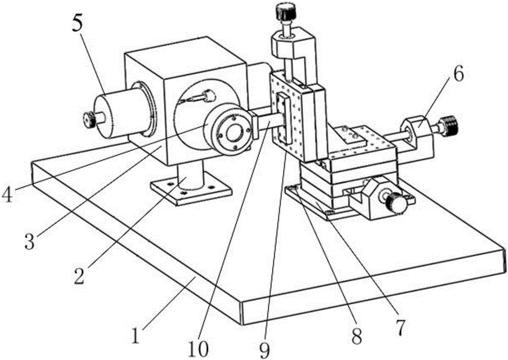
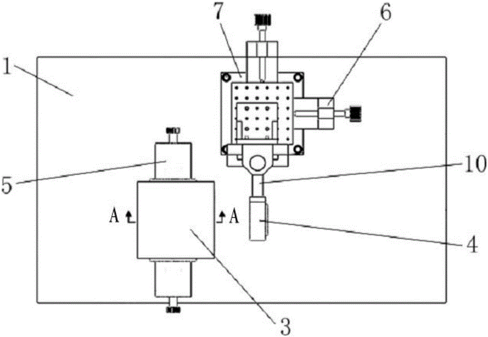
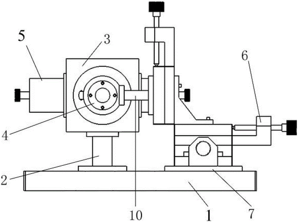
[0026] like Figure 1-Figure 3 As shown, the present invention relates to a focused shock wave excitation device for testing the dynamic characteristics of MEMS microstructures, comprising a substrate 1, and a manual three-axis displacement stage 6 and a support 2 are arranged on the substrate 1. The manual three-axis The displacement stage 6 is mounted on a base plate 7 , and the base plate 7 is fixed on the base plate 1 by screws 8 . A microstructure unit 4 is provided on the Z-axis slide 9 of the manual three-axis displacement stage 6;

[0027] like Figure 7-Figure 9 As shown, the micro-structure unit 4 includes a mounting sleeve 401 which is mounted on the Z-axis slide 9 through the horizontal support 10. The mounting sleeve 401 is provided with a stepped mounting hole. The MEMS microstructure 405 is installed on the structure mounting plate 407; the microstructure mounting plate 407 is fixed on the annular plane at the bottom of the mounting hole through the screws 406...


PUM


Abstract

The present invention discloses a focused shock wave excitation device for the dynamic feature testing of the microstructure of an MEMS (micro-electromechanical system). The device includes a substrate, a manual tri-axial displacement table and a supporting seat; the Z-axis slide plate of the manual tri-axial displacement table is provided with a microstructure unit; the upper end of the supporting seat is provided with an ellipsoidal cavity of which the inner cavity is half of an ellipsoidal surface; the first focus of the ellipsoidal surface is located in the ellipsoidal cavity; two sides of the ellipsoidal cavity are symmetrically provided with two pin electrode units; the tips of the two pin electrode units are located at the cross section of the first focus and point to the first focus; the microstructure of the MEMS is located at the second focus of the ellipsoidal surface; the two pin electrodes are electrically connected with the two poles of a high-voltage capacitor; a first air switch is arranged between one pin electrode and the high-voltage capacitor; the two poles of the high-voltage capacitor are electrically connected with a high-voltage power source; and the connection and disconnection of the high-voltage capacitor and the high-voltage power source are controlled by a second air switch. With the focused shock wave excitation device adopted, interference on a testing result caused by the vibration response of a base structure can be avoided, the non-contact excitation of the microstructure of the MEMS can be realized, an excitation effect is good, and the testing of the dynamic feature parameters of the microstructure can be facilitated.

Description

technical field [0001] The invention belongs to the technical field of micro-mechanical electronic systems, and particularly relates to a focused shock wave excitation device used for testing the dynamic characteristics of MEMS microstructures. Background technique [0002] Due to the advantages of low cost, small size and light weight, MEMS micro-devices have broad application prospects in many fields such as automobiles, aerospace, information communication, biochemistry, medical treatment, automatic control and national defense. For many MEMS devices, the micro-displacement and micro-deformation of their internal microstructures are the basis for the realization of device functions. Therefore, accurate testing of dynamic parameters such as amplitude, natural frequency, and damping ratio of these microstructures has become the key to developing MEMS products. important content. [0003] In order to test the dynamic characteristic parameters of the microstructure, the micr...

Claims


Application Information

Patent Timeline
Patent Type & Authority Applications(China)
IPC IPC(8): G01M7/02
CPCG01M7/022
Inventor 佘东生杨一柳魏泽飞赵玉峰刘继行
Owner BOHAI UNIV
Why Eureka
Try Eureka